Reference Design
R
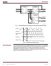
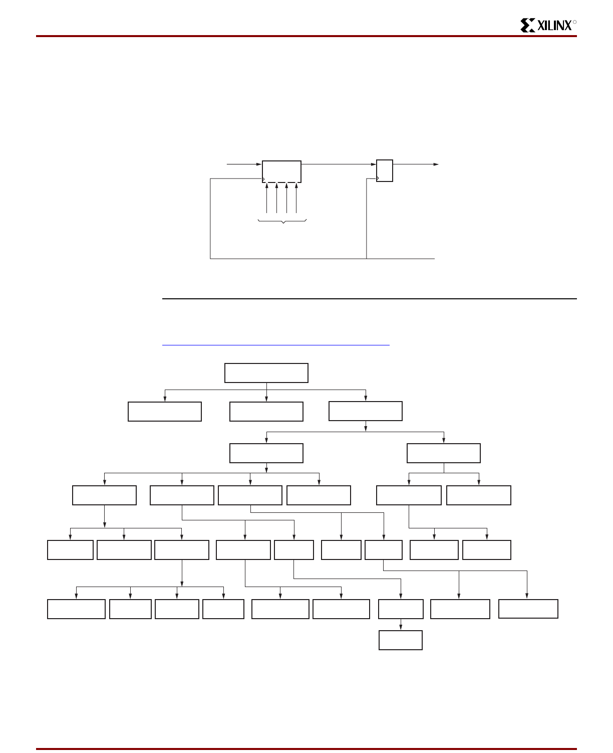
The ctrl_RdEn signal is required to validate read data because the DDR2 SDRAM devices do
not provide a read valid or read-enable signal along with read data. The controller generates
this read-enable signal based on the CAS latency and the burst length. This read-enable signal
is input to an SRL16 (LUT-based shift register). The number of register stages required to align
the read-enable signal to the ISERDES read data output is determined during calibration. One
read-enable signal is generated for each data byte. Figure 10 shows the read-enable logic
block diagram.
Reference
Design
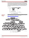
Figure 11 shows the hierarchy of the reference design. The mem_interface_top is the top-level
module. This reference design is available on the Xilinx website at:
http://www.xilinx.com/bvdocs/appnotes/xapp721.zip
.
Figure 10: Read-Enable Logic
x721_10_113005
CLKdiv_90
ctrl_RdEn
ctrl_RdEn_div0
Number of Register Stages
Selected During Calibration
SRL16
srl_out
FD
Figure 11: Reference Design Hierarchy
mem_Interface_top
idelay_ctrl
ddr2_controllerdata_pathuser_interfaceiobs
X721_11_113005
infrastructure
top test_bench
main
backend_rom cmp_rd_data
addr_gen data_gen_16tap_logicdata_writerd_databackend_fifosdatapath_iobscontroller_iobs
rd_wr_addr_fifo wr_data_fifo_16 rd_data_fifo tap_ctrl
infrastr_iobs
v4_dqs_iobv4_dm_iobidelay_rd_en_io v4_dq_iob
RAM_D
data_tap_inc
March 2006 Memory Interfaces Solution Guide 65


