


Chapter 4 135
Chipset POST Codes
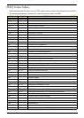
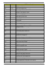
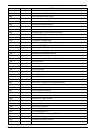
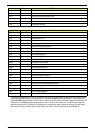
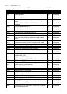
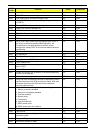
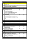
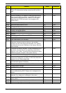
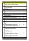
The following table details the Chipset POST codes and components used in the POST.
POST Code Function Phase Component
0xA0 MRC Entry PEI chipset/MRC
0x01 Enable MCHBAR PEI chipset/MRC
0x02 Check ME existence PEI chipset/MRC
0x03 Check for DRAM initialization interrupt and reset fail PEI chipset/MRC
0x04 Determine the system Memory type based on first populated
socket
PEI chipset/MRC
0x05 Verify all DIMMs are DDR2 and SO-DIMMS, which are
unbuffered
PEI chipset/MRC
0x06 Verify all DIMMs are Non-ECC PEI chipset/MRC
0x07 Verify all DIMMs are single or double sided and not mixed PEI chipset/MRC
0x08 Verify all DIMMs are x8 or x16 width PEI chipset/MRC
0x09 Calculate number of Row and Column bits PEI chipset/MRC
0x10 Calculate number of banks for each DIMM PEI chipset/MRC
0x11 Determine raw card type PEI chipset/MRC
0x12 Find a common CAS latency between the DIMMS and the
MCH
PEI chipset/MRC
0x13 Determine the memory frequency and CAS latency to program PEI chipset/MRC
0x14 Determine the smallest common timing value for all DIMMS PEI chipset/MRC
0x17 Power management resume PEI chipset/MRC
0x18 Program DRAM type (DDR2/DDR3) and Power up sequence PEI chipset/MRC
0x19 Program the correct system memory frequency PEI chipset/MRC
0x20 Program the correct Graphics memory frequency PEI chipset/MRC
0x21 Early DRC initialization PEI chipset/MRC
0x22 Program the DRAM Row Attributes and DRAM Row Boundary
registers PRE JEDEC.
PEI chipset/MRC
0x23 Program the RCOMP SRAM registers PEI chipset/MRC
0x24 Program DRAM type (DDR2/DDR3) and Power up sequence PEI chipset/MRC
0x25 Program the DRAM Timing PEI chipset/MRC
0x26 Program the DRAM Bank Architecture register PEI chipset/MRC
0x27 Enable all clocks on populated rows PEI chipset/MRC
0x28 Program MCH ODT PEI chipset/MRC
0x29 Program tRD PEI chipset/MRC
0x30 Miscellaneous Pre JEDEC steps PEI chipset/MRC
0x31 Program clock crossing registers PEI chipset/MRC
0x32 Program the Egress port timings PEI chipset/MRC
0x33 Program the Memory IO registers PEI chipset/MRC
0x34 Perform steps required before JEDEC PEI chipset/MRC
0x35 Perform JEDEC memory initialization for all memory rows PEI chipset/MRC
0x36 Setup DRAM control register for normal operation and enable PEI chipset/MRC
0x37 Do ZQ calibration for DDR3 PEI chipset/MRC
0x38 Perform final Dra/Drb programming, Set the mode of operation
for the memory channels
PEI chipset/MRC