


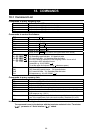
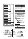
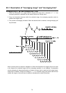

72
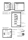
Pin assignments and I/O logic
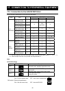
Output pin assignments Input pin assignments
Pin No. Signal Pin No Signal
26 1
7
BUSY
27 2
9
RE-ZERO
28 4
5
ON/OFF
Switch
29 8
10
0
3
Input signal GND
39 1
11
Not used (Reserved)
40 2
41 4
42 8
10
1
・The pins, which are not specified, have no
connection. (Pins 2, 4, 6, 8, 10, 36. 38)
12 1
Output logic
13 2
Factory settings
14 4
When State
15 8
10
2
Data 1 ON
16 1
Polarity Positive or zero display ON
17 2
Stability Stabilization indicator ON ON
18 4 Over e, -e display ON
19 8
10
3
Strobe Data receiving enabled* ON
20 1 Status Weighing ON
21 2 *Data refresh when OFF→ON
22 4
23 8
10
4
46 1
47 2
48 4
49 8
10
5
24 1
• All output, open collector; withstand
voltage 30 V; no pull-up resistor; low-level
output current 48 mA
• Output logic of data, status, and strobe
can be switched individually in the function
table bcd.
25 2
30 4
31 8
10
6
32 1
33 2
34 4
35 8
10
7
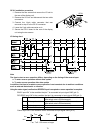
Data
50 Polarity
45 Stability
44 Over
State
37 Status
43 Strobe
Control
signal
1 Output signal GND
Input logic
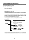
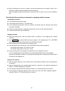
Housing Shield
BUSY Data will be held during ON
(when connected to input signal
GND).
Input by
switch
Valid when ON (when connected
to input signal GND).
• All input, no voltage contact or open
collector (connected to 5 V internally)
Balance interior
0
7
Output pins
FG
BCD signals
Pin 1
BCD signals
(Data from 10 -1 to 10 -8, Polarity,
Stability, OVER, Status, Strobe)
BCD signal ground
Output signal GND
Use a shielded cable.
(LS06)
Housing (Cable shield)
Balance interior
CPU
i
nput
terminal
Use a shielded cable.
Housing (Cable shield)
When a photocoupler is used
RE-ZERO
ON/OFF
BUSY
Input signal GND
11 Not used
(Reserved)
5 (Input terminal)
9 (Input terminal)
7 (Input terminal)
3
FG
(Upon switch-ON, make the voltage
between the input terminal and the
input signal GND terminal 0.2V or less)
When a switch is used
(1)
(2)
5,9 or 7 pin
Input signal GND
22k
Ω
10k
Ω
10k
Ω
820
Ω
5V
820
Ω
820
Ω
820
Ω
22k
Ω
5V 5V 5V
5,9 or 7 pin
Input signal GND