


34
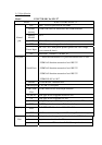
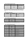
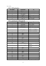
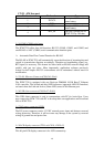
JP 3 : LCD signal voltage level select
Pin Number Pin function Ps.
1 SYS_VCC +5V
2 LCD_VCC
power of LCD-signal
buffers
3 VCC3P3
+3.3V. VCC3P3 will
change to 0V when
system enter sleep mode.
Note: when User wants to use CN18 (40 pin TTL level LCD signal) to drive LCD
panel, user needs to setup this pin header. If the LCD panel signal is 3.3V then set the
2.00mm jumper at 1-2 pin of JP3; if the LCD panel signal is 5V then set the jumper at
2-3 pin.
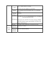
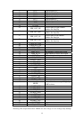
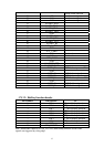
JP 4 : Power switch header
Pin Number Pin function Ps.
1 POW_SW_P connect to power switch
positive pole
2 POW_SW_N connect to power switch
negative pole
Note: Only pin 1 is shorted with pin 2 of JP4, the system power is on.
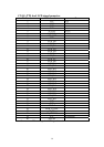
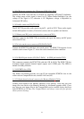
CN 1 : PCMCIA accessing status port
Pin Number Pin Function Ps.
1 Resv.
2 Resv.
3 PCM_RDY
4 PCM_VR
Note: If user wants to know the accessing status of PCMCIA slot, user can directly
connect the LED positive pole to 4
th
pin and negative pole to 3
rd
pin.
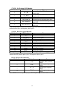
CN 3 : multi-function I/O header (I)
Pin Number Pin Function Ps.
1 Resv.
2 Resv.
3 Resv.
4 Resv.
5 Resv.
6 Resv.
7 DI 0* Digital input bit 0.
8 DO 0* Digital output bit 0.
9 DI 1* Digital input bit 1.
10 DO1* Digital output bit 1.
11 DI 2* Digital input bit 2.
12 DO2* Digital output bit 2.
13 DI 3* Digital input bit 3.
14 DO3* Digital output bit 3.
15 DI 4* Digital input bit 4.
16 DO 4* Digital output bit 4.