


P/E-P55T2P4D User’s Manual 37
IV. BIOS SOFTWARE
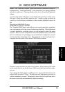
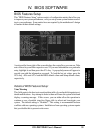
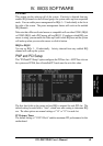
IV. BIOS
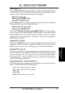
(Chipset Features)
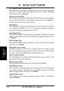
[DRAM and ECC]
If all your DRAM modules have parity chips (e.g. 8 chips + 4 parity chips), they are
considered 36bits. This motherboard sums the memory per bank and therefore two
modules will give 72bits and the following will be displayed:
DRAM are 72 bits wide
Memory parity SERR# (NMI):
DRAM ECC/PARITY Select:
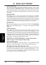
If your DRAM modules do not have parity chips (e.g. 8 chips), they are considered
32bits and the following will be displayed instead:
DRAM are 64 (not 72) bits wide
Memory parity SERR# (NMI):
The default of Disabled for Memory parity SERR# (NMI) will not show memory
errors on your monitor. When using parity DRAM modules, you can select from the
default of Parity or ECC (Error Checking and Correcting) to correct 1 bit memory
errors that may occur in the memory. (See pages 12-13 for more information on
DRAM memory modules.)
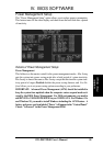
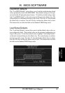
Onboard FDC Controller
The default of Enabled allows you to connect your floppy disk drives to the onboard
floppy drive connector instead of a separate controller card. If you want to use a
different controller card to connect the floppy drives, set this field to Disabled.
Onboard FDC Swap A: B:
This field reverses the drive letter assignments of your floppy disk drives. If you
want to switch drive letter assignments, set this field to Swap AB, otherwise leave on
default of No Swap. This works separately from the BIOS FEATURES SETUP
"Swap Floppy Drive." This is functionally the same as physically interchanging the
connectors of the floppy disk drives.
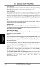
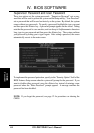
Onboard Serial Port 1 / Onboard Serial Port 2
These fields control the assignments for the motherboard’s two onboard serial con-
nectors. The following lists the available options:
COM1, 3F8H (Onboard Serial Port 1 default)
COM2, 2F8H (Onboard Serial Port 2 default)
COM3, 3E8H
COM4, 2E8H
Disabled (Disables the onboard serial ports)