


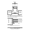

Documentation Number 232OPSDA1397 Manual 15
B&B Electronics -- PO Box 1040 -- Ottawa, IL 61350
PH (815) 433-5100 -- FAX (815) 433-5105
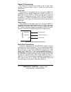
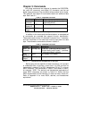
Chapter 4: A/D
This chapter will deal with the various A/D channels and
manipulating the data obtained from them.
Sampling Rate
The A/D converter has a conversion time around 10
microseconds, however, the actual sampling rate is limited by the
serial communications. The actual sampling rate for a single
channel is around 120 samples per second (9600 baud). This rate
drops to around 41 samples per second when sampling all of the
channels. When reading an A/D input, the 232OPSDA takes four
readings and returns the average (0.5 and greater are rounded up)
of these readings. This averaging helps filter out noise.
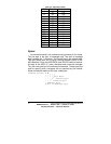
A/D Converter Range
The actual A/D converter chip in the 232OPSDA is a 12 bit A/D
converter that can read analog voltages between 0 and 5VDC.
However, the 232OPSDA contains signal conditioning circuitry that
allows you to measure voltages from 0 to 10VDC (Gain = 0.5) as
well as other ranges. In the following sections, each channel
configuration will be covered.
Non-buffered 0 to 5VDC A/D Inputs
The 232OPSDA has two non-buffered 0 to 5V inputs. They are
A/D 4 on Terminal Block 4 and A/D 5 on Terminal Block 5. The
voltage applied to the Terminal Blocks is the voltage that is read by
the A/D converter chip. The driving source impedance should be
less than 1KΩ for these two channels.
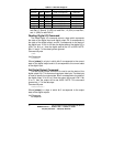
Buffered 0 to 5V A/D Inputs
The 232OPSDA has two buffered 0 to 5V inputs. They are A/D 1
on Terminal Block 1 and A/D 2 on Terminal Block 2. An operational
amplifier is setup as a voltage follower to buffer the A/D converter
from the source of the voltage. The input resistance of each of these
channels is 1TΩ. This allows you to have a large source impedance.
Both A/D 1 and A/D 2 are set up as voltage followers with a gain
of 1 when they leave the factory. However, the voltage follower for
A/D 1 (TB 1) has spaces for optional through hole resistors. This
allows you to reconfigure A/D 1 into a non-inverting amplifier
configuration. A non-inverting amplifier can have a gain greater than
1. See the circuit schematic in Figure B.1 and board layout in Figure
B.2 in Appendix B. To change the voltage follower into a non-