


Documentation Number 232OPSDA1397 Manual 17
B&B Electronics -- PO Box 1040 -- Ottawa, IL 61350
PH (815) 433-5100 -- FAX (815) 433-5105
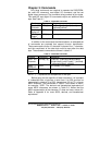
The signal conditioning circuit for this A/D input channel has been
designed to be easily modified. In the original configuration, R5 and
R6 are left OPEN (they are not present). These two spaces are
provided if you need a different gain. Reducing the gain of this non-
inverting amplifier allows you to measure currents up to 100mA, and
increasing the gain allows you to read much smaller currents with
greater accuracy. See the circuit schematic in Figure B.1 and board
layout in Figure B.2 in Appendix B.
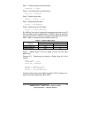
To change the gain of this non-inverting amplifier, remove R8
and R9, and calculate values for R4 and R5 using the equation
below.
Gain
V
LoopCurrent
R
R
=
×
=+
0
10
1
5
4
NOTE: V
0
is the voltage read by the A/D converter and (10 x loop
current) is the voltage drop across the 10Ω resistor. R4 and R5
should be chosen so that V
0
does not exceed 5.00VDC.
NOTE: Decreasing the gain allows you to measure larger currents,
but the maximum current that can be read is 100mA. The 100mA
limit is due to the power rating of the 10Ω resistor (0.125W).
NOTE: When using the 4-20mA current loop input, A/D 1 - A/D 5
should be connected to the terminal block labeled GND.