


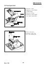
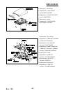
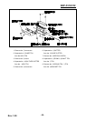
Rev. 1.00
- 44 -
SRP-F310/312
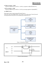
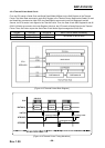
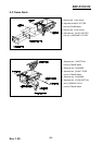
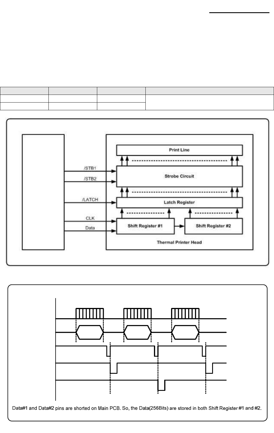
4-3-9 Thermal Printer Head Circuit
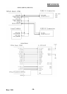
First, the CPU sends a Serial Clock and Serial Data 256bits(32Bytes) to the Shift Register of the Thermal
Printer. The Serial Data are stored to each Shift Register in the Thermal Printer. Because the Data#1 Pin and
the Data#2 pin are shorted on Main PCB, the Data(256bits) are stored in both Shift Register#1 and #2.
Second, the CPU send a Latch Signal to the Thermal Printer. Then, the Data of both Shift Register#1 and #2
(256*2=512bits) are moved to the Latch Register. After that, the CPU sends a Strobe Signal to the Thermal
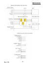
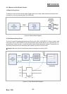
Printer. Then, the Printer outputs the Serial Data. Each Strobe Signal manages the Printer Dot.
STB No. DOT No. DOTs/STB SRP-F310/312 Strobe Processing
STB1 1 ~ 256 256
STB2 257 ~ 512 256
The content of data is same.
[Figure 4-13 Thermal Printer Block Diagram]
/LATCH
STROBE1
STROBE2
DATA#1,2
CLK
256bits 256bits 256bits
Printing(1~256) Printing(1~256)
Printing(257~512)
256 CLK
[Figure 4-14 Thermal Printer Timing Waveform]
CPU
SPEAr300