


4–4 Functional Description
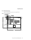
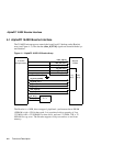
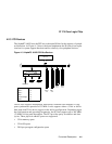
21174 Core Logic Chip
The 21174 chip provides the following functions:
• Serves as the interface between the 21164PC microprocessor, main memory
(addressing and control), and the PCI bus. A three-entry CPU instruction queue
is implemented to capture commands should the memory or I/O port be busy.
• Provides control to the Quick Switch chips to isolate the L2 cache from the main
memory bus during private reads and writes.
• Generates the clocks, row, and column addresses for the SDRAM DIMMs, as
well as all of the memory control signals (RAS, CAS, WE). All of the required
SDRAM refresh control is contained in the 21174.
• Provides all the logic to map 21164PC noncacheable addresses to PCI address
space, as well as all the translation logic to map PCI DMA addresses to system
memory.
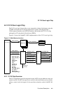
Two DMA conversion methods are supported:
• Direct mapping, in which a base offset is concatenated with the PCI address.
• Scatter-gather mapping, which maps an 8KB PCI page to any 8KB memory
page. The 21174 contains an eight-entry scatter-gather translation lookaside
buffer (TLB), where each entry holds four consecutive page table entries (PTEs).
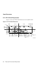
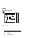
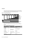
4.2.2 Main Memory Interface
Quick Switches provide the interface between the 21164PC/L2 cache (data_h[127:0])
and the memory/21174 (mem_data_h[127:0]). The AlphaPC 164SX supports four
168-pin unbuffered 72-bit or 64-bit SDRAM DIMM modules. Even parity is generated
on the PCI bus.
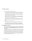
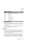
The AlphaPC 164SX supports a maximum of 512MB of main memory. The memory
is organized as two banks. Table 1–1 lists total memory options along with the corre-
sponding DIMM sizes required. All CPU cacheable memory accesses and PCI DMA
accesses are controlled and routed to main memory by the 21174 core logic chip.
The AlphaPC 164SX implements the alternate memory mode for SDRAM RAS
and CAS control signals. Alternate memory mode is explained in the 21174 Core
Logic Chip Technical Reference Manual.