


4–14 Functional Description
Reset and Initialization
The 21164PC microprocessor produces the divided clock output signal sys_clk_out1
that drives the CY2308 PLL clock-driver chip. This clock provides the references to
synchronize the 21164PC microprocessor and the 21174 chip. The 21174 provides
the system memory and I/O (PCI) clock references. It also provides system-level
clocking to DIMMs, PCI slots, the PCI-ISA bridge, the PCI ID controller, and the
PCI arbiter.
A 14.3-MHz crystal produces the signal 14mhz_out. This signal is delivered to the
FDC37C669 combination controller for the diskette data separator and other I/O
clocks. The combination controller produces output clock osc, which is then deliv-
ered to the two ISA slots and the PCI-to-ISA bridge for synchronization.
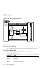
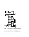
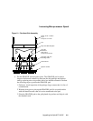
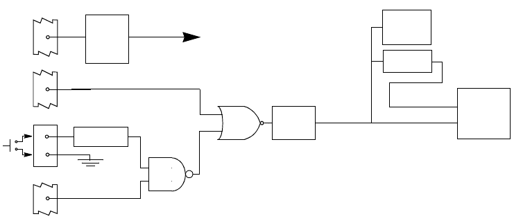
4.6 Reset and Initialization
A TL7702B power monitor senses the +3.3-V rail to ensure that it is stable before
+2.5 V is applied to the 21164PC. In normal operation, if the +3.3-V rails fall below
+2.5 V, the power monitor enables shdn_l, which turns off the +2.5-V regulator.
An external reset switch can be connected to J20. The reset function initializes the
21164PC and the system logic. The p_dcok signal provides a full system initializa-
tion, equivalent to a power-down and power-up cycle.
In addition, the fan sense signal (fan_ok_l) is logically ORed with the reset switch
output and the p_dcok signal. This signal (monitor_reset_l) is used to reset the
MAX708R +3.3-V monitor. If any of the signals become asserted, or if +3.3 V drops
to +2.5 V, then dc_ok_h is deasserted, which causes a system reset.
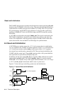
Figure 4–7 shows the logic controlling system reset and initialization.
Figure 4–7 System Reset and Initialization
2
3
4
8
Sense
shdn_l
To +2.5-V Regulator
Debounce
J2
J14
J20
J2
Reset
Switch
fan_ok_l
p_dcok
3-V
Monitor
dc_ok_h
PCI-ISA
Bridge
21174
cpu_reset
21164PC
+3.3 V
Fan
Sensor
Power
Supply