


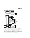

Functional Description 4–9
Interrupts
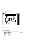
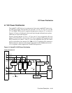
4.3.4 Flash ROM Address Map
After reset, the flash ROM is set to location 0. The 21174 supports cache fills and
uncacheable reads from the flash ROM (that is, the 21174 does multiple reads to the
flash ROM to assemble full octawords). The 21164PC can start executing directly
from the flash ROM.
Once the boot code that was stored in the flash ROM has been executed, and mem-
ory has been initialized, the flash ROM is mapped to locations
87.C000.000–87.FFFF.FFFF.
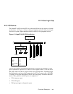
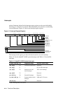
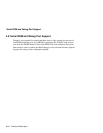
4.4 Interrupts
Interrupts and general-purpose inputs are acquired by the 21174 through a free-
running 32-bit external shift register. The int_sr_load_l signal is asserted low to load
the interrupts into the shift register. The int_clk signal clocks the shift register con-
tents into the 21174 through the int_sr_in pin. The shift register operates continu-
ously at a rate of ¼ the chipset clock rate.
The state of each interrupt can be read through the interrupt request register. Note
that the state of the interrupts will persist in the interrupt request register for up to
3 µs after the interrupt has been deasserted at the shift register. If the interrupt bit in
the interrupt request register is not promptly cleared, a second interrupt might be
taken before the shift register scans the deasserted value into the interrupt request
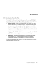
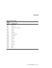
070 CMOS RAM address and NMI mask register
080-08F DMA page registers
0A0-0A1 8259 PIC #2
0C0-0DF 8237 DMA #2
2F8-2FF Serial port—COM2
370-377 Secondary diskette (floppy)
3BC-3BF Parallel port—LPT1
3F0-3F7 Primary diskette (floppy)
3F8-3FF Serial port—COM1
Table 4–1 ISA I/O Address Map
(Sheet 2 of 2)
Range (hex) Usage