


PRELIMINARY
CY14B101P
Document #: 001-44109 Rev. *B Page 10 of 32
When WP
pin is LOW and WPEN is set to “1”, any modifications
to status register are disabled. Therefore, the memory is
protected by setting the BP0 and BP1 bits and the WP pin inhibits
any modification of the status register bits, providing hardware
write protection.
Note WP going LOW when CS is still LOW has no effect on any
of the ongoing write operations to the status register.
Table 6 summarizes all the protection features provided in the
CY14B101P.
Memory Access
All memory accesses are done using the READ and WRITE
instructions. These instructions cannot be used while a STORE
or RECALL cycle is in progress. A STORE cycle in progress is
indicated by the RDY
bit of the status register and the HSB pin.
Read Sequence (READ)
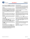
The read operations on CY14B101P are performed by giving the
instruction on Serial Input pin (SI) and reading the output on
Serial Output (SO) pin. The following sequence needs to be
followed for a read operation: After the CS
line is pulled LOW to
select a device, the read opcode is transmitted through the SI
line followed by three bytes of address. The Most Significant
address byte contains A16 in bit 0 and other bits as don’t cares.
Address bits A15 to A0 are sent in the following two address
bytes. After the last address bit is transmitted on the SI pin, the
data (D7-D0) at the specific address is shifted out on the SO line
on the falling edge of SCK. Any other data on SI line after the last
address bit is ignored.
CY14B101P allows reads to be performed in bursts through SPI
which can be used to read consecutive addresses without
issuing a new READ instruction. If only one byte is to be read,
the CS
line must be driven HIGH after one byte of data comes
out. However, the read sequence may be continued by holding
the CS line LOW and the address is automatically incremented
and data continues to shift out on SO pin. When the last data
memory address (0x1FFFF) is reached, the address rolls over to
0x0000 and the device continues to read.
Write Sequence (WRITE)
The write operations on CY14B101P are performed through the
Serial Input (SI) pin. To perform a write operation CY14B101P, if
the device is write disabled, then the device must first be write
enabled through the WREN instruction. When the writes are
enabled (WEN = ‘1’), WRITE instruction is issued after the falling
edge of CS
. A WRITE instruction constitutes transmitting the
WRITE opcode on SI line followed by 3-bytes address sequence
and the data (D7-D0) which is to be written. The Most Significant
address byte contains A16 in bit 0 with other bits being don’t
cares. Address bits A15 to A0 are sent in the following two
address bytes.
CY14B101P allows writes to be performed in bursts through SPI
which can be used to write consecutive addresses without
issuing a new WRITE instruction. If only one byte is to be written,
the CS
line must be driven HIGH after the D0 (LSB of data) is
transmitted. However, if more bytes are to be written, CS
line
must be held LOW and address incremented automatically. The
following bytes on the SI line are treated as data bytes and
written in the successive addresses. When the last data memory
address (0x1FFFF) is reached, the address rolls over to 0x0000
and the device continues to write.
The WEN bit is reset to “0” on completion of a WRITE sequence.
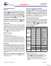
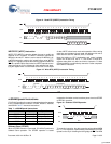
Table 6. Write Protection Operation
WPEN WP WEN
Protected
Blocks
Unprotected
Blocks
Status
Register
X X 0 Protected Protected Protected
0 X 1 Protected Writable Writable
1 LOW 1 Protected Writable Protected
1 HIGH 1 Protected Writable Writable
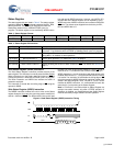
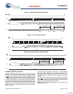
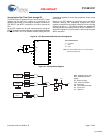
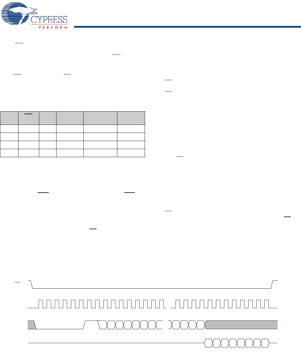
Figure 10. Read Instruction Timing
~
~
CS
SCK
SO
012345 67
0
765432
1
20212223012345 67
MSB LSB
Data
SI
~
~
Op-Code
0000001
0000
0 0
1
0
A16
A3
A1A2
A0
17-bit Address
MSB LSB
D0
D1
D2
D3
D4
D5
D6
D7
[+] Feedback