


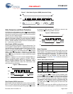
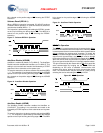

PRELIMINARY
CY14B101P
Document #: 001-44109 Rev. *B Page 5 of 32
master is the opcode. Following the opcode, any addresses and
data are then transferred. The CS must go inactive after an
operation is complete and before a new opcode can be issued.
The commonly used terms used in SPI protocol are given below:
SPI Master
The SPI Master device controls the operations on a SPI bus. An
SPI bus may have only one master with one or more slave
devices. All the slaves share the same SPI bus lines and master
may select any of the slave devices using the Chip Select pin.
All the operations must be initiated by the master activating a
slave device by pulling the CS
pin of the slave LOW. The master
also generates the Serial Clock (SCK) and all the data trans-
mission on SI and SO lines are synchronized with this clock.
SPI Slave
SPI slave device is activated by the master through the Chip
Select line. A slave device gets the Serial Clock (SCK) as an
input from the SPI master and all the communication is
synchronized with this clock. SPI slave never initiates a
communication on the SPI bus and acts on the instruction from
the master.
CY14B101P operates as a slave device and may share the SPI
bus with multiple CY14B101P devices or other SPI devices.
Chip Select (CS
)
For selecting any slave device, the master needs to pull down
the corresponding CS
pin. Any instruction can be issued to a
slave device only while the CS
pin is LOW.
The CY14B101P is selected when the CS
pin is LOW. When the
device is not selected, data through the SI pin is ignored and the
serial output pin (SO) remains in a high impedance state.
Note A new instruction must begin with the falling edge of Chip
Select (CS
). Therefore, only one opcode can be issued for each
active Chip Select cycle.
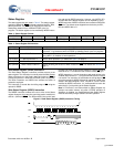
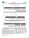
Serial Clock (SCK)
Serial clock is generated by the SPI master and the communi-
cation is synchronized with this clock after CS
goes LOW.
CY14B101P allows SPI modes 0 and 3 for data communication.
In both these modes, the inputs are latched by the slave device
on the rising edge of SCK and outputs are issued on the falling
edge. Therefore, the first rising edge of SCK signifies the arrival
of first bit (MSB) of SPI instruction on the SI pin. Further, all data
inputs and outputs are synchronized with SCK.
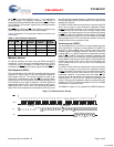
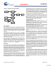
Data Transmission SI/SO
SPI data bus consists of two lines, SI and SO, for serial data
communication. The SI is also referred to as MOSI (Master Out
Slave In) and SO is referred to as MISO (Master In Slave Out).
The master issues instructions to the slave through the SI pin,
while slave responds through the SO pin. Multiple slave devices
may share the SI and SO lines as described earlier.
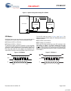
CY14B101P has two separate pins for SI and SO which can be
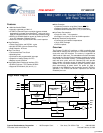
connected with the master as shown in Figure 3 on page 6.
Most Significant Bit (MSB)
The SPI protocol requires that the first bit to be transmitted is the
Most Significant Bit (MSB). This is valid for both address and
data transmission.
CY14B101P requires a 3-byte address for any read or write
operation. However, since the actual address is only 17 bits, it
implies that the first seven bits, which are fed in, are ignored by
the device. Although these seven bits are ‘don’t care’, Cypress
recommends that these bits are treated as 0s to enable
seamless transition to higher memory densities.
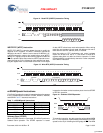
Serial Opcode
After the slave device is selected with CS
going LOW, the first
byte received is treated as the opcode for the intended operation.
CY14B101P uses the standard opcodes for memory accesses.
In addition to the memory accesses, CY14B101P provides
additional opcodes for the nvSRAM specific functions: STORE,
RECALL, AutoStore Enable, and AutoStore Disable. Refer to
Table 2 on page 7 for details on opcodes.
Invalid Opcode
If an invalid op-code is received, the op-code is ignored and the
device ignores any additional serial data on the SI pin. and no
valid data is sent out on the SO pin. Opcode for a new instruction
is recognized only after the next falling edge of CS
.
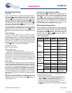
Status Register
CY14B101P has an 8-bit status register. The bits in the status
register are used to configure the SPI bus. These bits are
described in the Table 4 on page 8.
[+] Feedback