


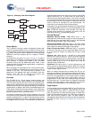
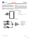
PRELIMINARY
CY14B101P
Document #: 001-44109 Rev. *B Page 20 of 32
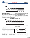
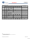
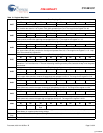
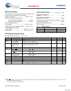
0x07
WatchDog Timer
D7 D6 D5 D4 D3 D2 D1 D0
WDS WDW WDT
WDS Watchdog Strobe. Setting this bit to 1 reloads and restarts the watchdog timer. Setting the bit to 0 has no effect. The bit
is cleared automatically after the watchdog timer is reset. The WDS bit is write only. Reading it always returns a 0.
WDW Watchdog Write Enable. Setting this bit to 1 disables any WRITE to the watchdog timeout value (D5–D0). This enables
the user to set the watchdog strobe bit without disturbing the timeout value. Setting this bit to 0 allows bits D5–D0 to
be written to the watchdog register when the next write cycle is complete. This function is explained in more detail in
Watchdog Timer on page 15.
WDT Watchdog timeout selection. The watchdog timer interval is selected by the 6-bit value in this register. It represents a
multiplier of the 32 Hz count (31.25 ms). The range of timeout value is 31.25 ms (a setting of 1) to 2 seconds (setting
of 3 Fh). Setting the watchdog timer register to 0 disables the timer. These bits can be written only if the WDW bit was
set to 0 on a previous cycle.
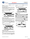
0x06
Interrupt Status/Control
D7 D6 D5 D4 D3 D2 D1 D0
WIE AIE PFE 0 H/L P/L 0 0
WIE Watchdog Interrupt Enable. When set to 1 and a watchdog timeout occurs, the watchdog timer drives the INT pin and
the WDF flag. When set to 0, the watchdog timeout affects only the WDF flag.
AIE Alarm Interrupt Enable. When set to 1, the alarm match drives the INT pin and the AF flag. When set to 0, the alarm
match only affects the AF flag.
PFE Power Fail Enable. When set to 1, the alarm match drives the INT pin and the PF flag. When set to 0, the power fail
monitor affects only the PF flag.
0 Reserved for future use
H/L HIGH/LOW. When set to 1, the INT pin is driven active HIGH. When set to 0, the INT pin is open drain, active LOW.
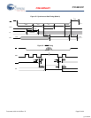
P/L Pulse/Level. When set to 1, the INT pin is driven active (determined by H/L) by an interrupt source for approximately
200 ms. When set to 0, the INT pin is driven to an active level (as set by H/L) until the flags register is read.
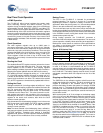
0x05
Alarm - Day
D7 D6 D5 D4 D3 D2 D1 D0
M 0 10s Alarm Date Alarm Date
Contains the alarm value for the date of the month and the mask bit to select or deselect the date value.
M Match. When this bit is set to 0, the date value is used in the alarm match. Setting this bit to 1 causes the match circuit
to ignore the date value.
0x04
Alarm - Hours
D7 D6 D5 D4 D3 D2 D1 D0
M 10s Alarm Hours Alarm Hours
Contains the alarm value for the hours and the mask bit to select or deselect the hours value.
M Match. When this bit is set to 0, the hours value is used in the alarm match. Setting this bit to 1 causes the match circuit
to ignore the hours value.
0x03
Alarm - Minutes
D7 D6 D5 D4 D3 D2 D1 D0
M 10s Alarm Minutes Alarm Minutes
Contains the alarm value for the minutes and the mask bit to select or deselect the minutes value.
M Match. When this bit is set to 0, the minutes value is used in the alarm match. Setting this bit to 1 causes the match
circuit to ignore the minutes value.
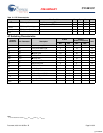
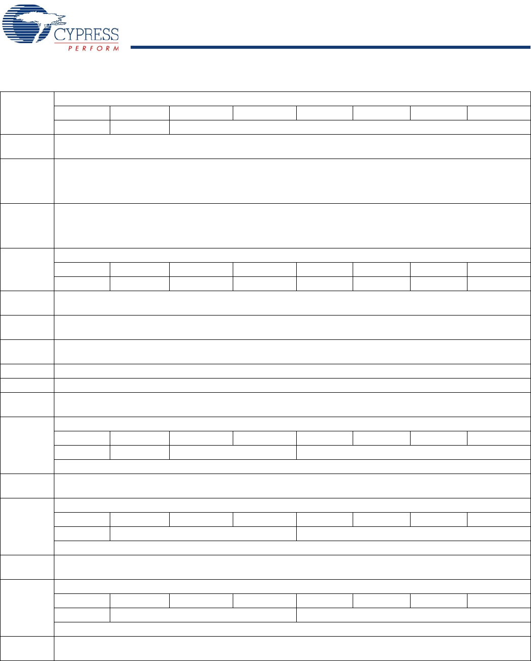
Table 10. Register Map Detail (continued)
[+] Feedback