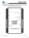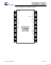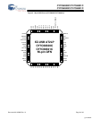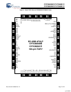
CY7C68300C/CY7C68301C
CY7C68320C/CY7C68321C
Document 001-05809 Rev. *A Page 11 of 42
Additional Pin Descriptions
The following sections provide additional pin information.
DPLUS, DMINUS
DPLUS and DMINUS are the USB signaling pins; they must
be tied to the D+ and D– pins of the USB connector. Because
they operate at high frequencies, the USB signals require
special consideration when designing the layout of the PCB.
See “General PCB Layout Recommendations For USB Mass
Storage Designs” on page 39 for PCB layout recommenda-
tions.
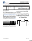
When RESET# is released, the assertion of the internal pull
up on D+ is gated by a combination of the state of the
VBUS_ATA_ENABLE pin, the value of configuration address
0x08 bit 0 (DRVPWRVLD Enable), and the detection of a
non-removable ATA/ATAPI drive on the IDE bus. See Tab le 2
for a description of this relationship.
SCL, SDA
The clock and data pins for the I
2
C port must be connected to
the configuration EEPROM and to 2.2K pull up resistors tied
to V
CC
. If no EEPROM is used in the design, the SCL and SDA
pins must still be connected to pull up resistors. The SCL and
SDA pins are active for several milliseconds at startup.
XTALIN, XTALOUT
The AT2LP requires a 24 MHz (
±100 ppm) signal to derive
internal timing. Typically, a 24 MHz (12 pF, 500 μW,
parallel-resonant, fundamental mode) crystal is used, but a 24
MHz square wave (3.3V, 50/50 duty cycle) from another
source can also be used. If a crystal is used, connect its pins
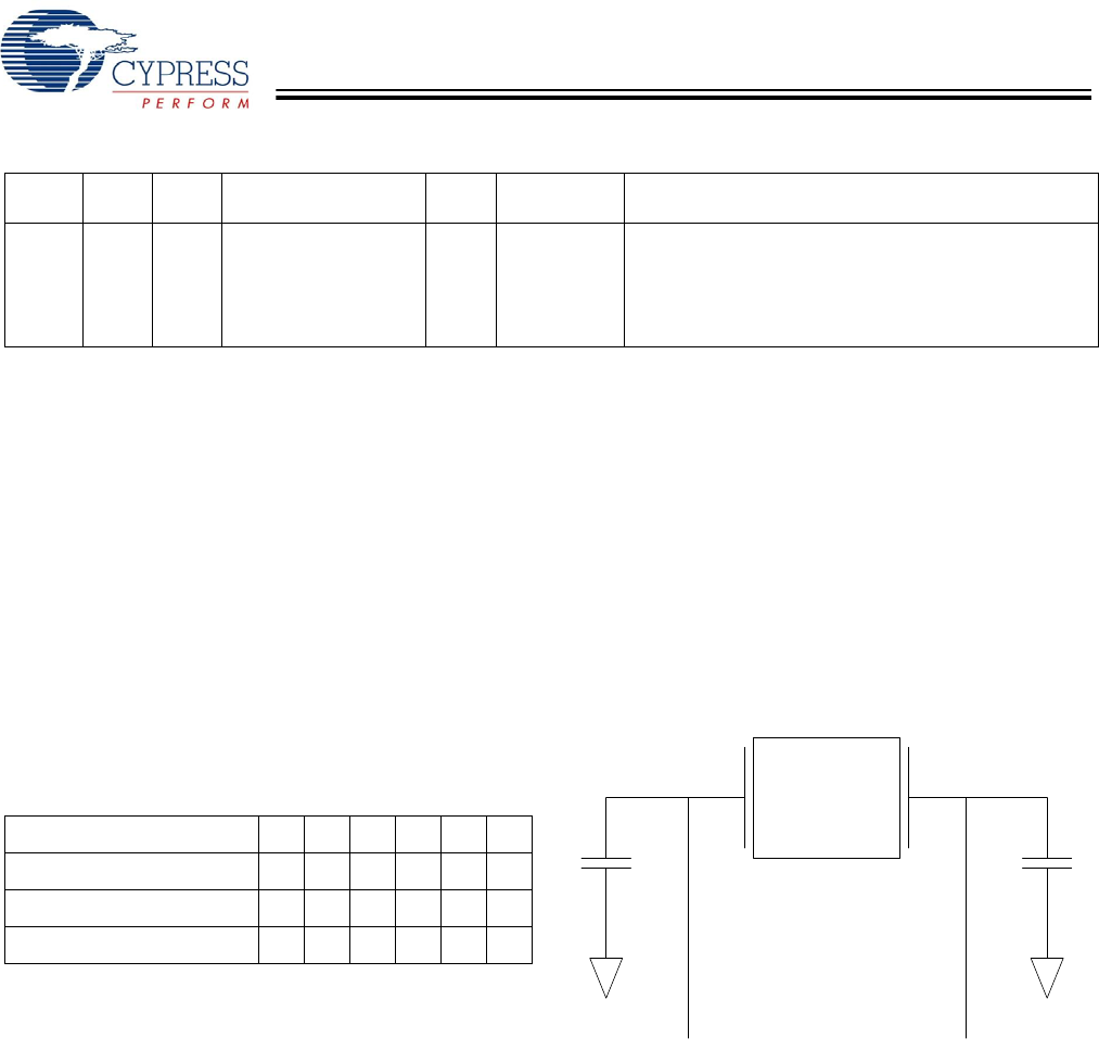
to XTALIN and XTALOUT, and also through 12 pF capacitors
to GND as shown in Figure 7. If an alternate clock source is
used, apply it to XTALIN and leave XTALOUT unconnected.
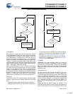
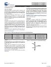
Figure 7. XTALIN/XTALOUT Diagram
100
[3]
54
[3]
5 ATAPUEN
(NC)
IO Bus-powered ATA pull up voltage source (see
“ATAPUEN” on page 14).
Alternate function: General purpose input when the
EEPROM configuration byte 8 has bit 7 set to ‘1’. The
input value is reported through EP1IN (byte 0, bit 2).
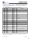
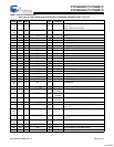
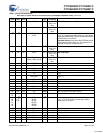
Table 1. AT2LP Pin Descriptions
Note: (Italic pin names denote pin functionality during CY7C68300A compatibility mode) (continued)
100
TQFP
56
QFN
56
SSOP
Pin Name
Pin
Type
Default State
at Startup
Pin Description
Table 2. D+ Pull Up Assertion Dependencies
VBUS_ATA_EN111100
DRVPWRVLD Enable Bit110011
ATA/ATAPI Drive Detected
YesNoYesNoYesNo
State of D+ pull up111000
24MHz Xtal
12pF
XTALIN XTALOUT
12pF
[+] Feedback


