CY7C68300C/CY7C68301C
CY7C68320C/CY7C68321C
Document 001-05809 Rev. *A Page 24 of 42
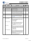
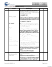
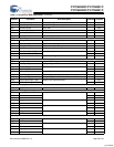
0x08 BUTTON_MODE Bit 7
Button mode (100-pin package only). Sets ATAPUEN,
PWR500# and DRVPWRVLD to become button inputs
returned on bits 2, 1, and 0 of EP1IN. This bit must be set to
‘0’ if the 56-pin packages are used.
0 = Disable button mode.
1 = Enable button mode.
0x78
SEARCH_ATA_BUS Bit 6
Search ATA bus after RESET to detect non-removable ATA
and ATAPI devices. Systems with only a removable device
(like CF readers) must set this bit to ‘0’. Systems with at least
one non-removable device must set this bit to ‘1’.
0 = Do not search for ATA devices.
1 = Search for ATA devices.
BIG_PACKAGE Bit 5
Selects the 100- or 56-pin package pinout configuration.
Using the wrong pinout may result in unpredictable behavior.
0 = Use 56-pin package pinout.
1 = Use 100-pin package pinout.
ATA_EN Bit 4
Drive ATA bus when AT2LP is in suspend. For designs in
which the ATA bus is shared between the AT2LP and
another ATA master (such as an MP3 player), the AT2LP
can place the ATA interface pins in a Hi-Z state when it
enters suspend. For designs that do not share the ATA bus,
the ATA signals must be driven while the AT2LP is in
suspend to avoid floating signals.
0 = Drive ATA signals when AT2LP is in suspend.
1 = Set ATA signals to Hi-Z when AT2LP is in suspend.
Reserved Bit 3
Reserved. This bit must be set to ‘0’.
Reserved Bit 2
Reserved. This bit must be set to ‘0’
Drive Power Valid Polarity Bit 1
Configure the logical polarity of the DRVPWRVLD input pin.
0 = Active LOW (‘connector ground’ indication)
1 = Active HIGH (power indication from device)
Drive Power Valid Enable Bit 0
Enable the DRVPWRVLD pin. When this pin is enabled, the
AT2LP enumerates a removable ATA device, like Compact-
Flash or MicroDrive, as the IDE master device. Enabling this
pin also affects other pins related to removable device
operation.
0 = Disable removable ATA device support.
1 = Enable removable ATA device support.
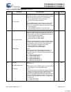
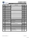
0x09 Reserved
General Purpose IO Pin
Output Enable
Bits 7:6
Reserved. Must be set to zero.
Bits 5:0
GPIO[5:0] Input and output control. GPIOs can be individ-
ually set as inputs or outputs using these bits.
0 = Hi-Z (pin is an input). The state of the signal connected
to GPIO input pins is reported in the SYSIRQ or HID data.
1 = Output enabled (pin is an output). The state of GPIO
output pins is controlled by the value in address 0x0A.
0x00
Table 11.Configuration Data Organization (continued)
Byte
Address
Configuration
Item Name
Configuration
Item Description
Required
Contents
Variable
Contents
[+] Feedback


