


CYV15G0404DXB
Document #: 38-02097 Rev. *B Page 28 of 44
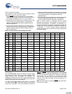
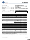
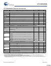
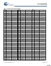
CYV15G0404DXB AC Electrical Characteristics
Parameter Description Min. Max Unit
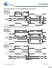
CYV15G0404DXB Transmitter LVTTL Switching Characteristics Over the Operating Range
f
TS
TXCLKx Clock Cycle Frequency 19.5 150 MHz
t
TXCLK
TXCLKx Period=1/f
TS
6.66 51.28 ns
t
TXCLKH
[20]
TXCLKx HIGH Time 2.2 ns
t
TXCLKL
[20]
TXCLKx LOW Time 2.2 ns
t
TXCLKR
[20, 21, 22]
TXCLKx Rise Time 0.2 1.7 ns
t
TXCLKF
[20, 21, 22]
TXCLKx Fall Time 0.2 1.7 ns
t
TXDS
Transmit Data Set-up Time to TXCLKx↑ (TXCKSELx ≠ 0) 2.2 ns
t
TXDH
Transmit Data Hold Time from TXCLKx↑ (TXCKSELx ≠ 0) 1.0 ns
f
TOS
TXCLKOx Clock Frequency = 1x or 2x REFCLKx Frequency 19.5 150 MHz
t
TXCLKO
TXCLKOx Period=1/f
TOS
6.66 51.28 ns
t
TXCLKOD
TXCLKO Duty Cycle centered at 60% HIGH time –1.9 0 ns
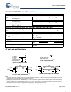
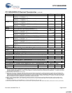
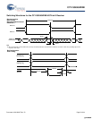
CYV15G0404DXB Receiver LVTTL Switching Characteristics Over the Operating Range
f
RS
RXCLKx± Clock Output Frequency 9.75 150 MHz
t
RXCLKP
RXCLKx± Period = 1/f
RS
6.66 102.56 ns
t
RXCLKD
RXCLKx± Duty Cycle Centered at 50% (Full Rate and Half Rate when
RXCKSELx = 0)
–1.0 +1.0 ns
t
RXCLKR
[20]
RXCLKx± Rise Time 0.3 1.2 ns
t
RXCLKF
[20]
RXCLKx± Fall Time 0.3 1.2 ns
t
RXDv–
[23]
Status and Data Valid Time to RXCLKx± (RXRATEx = 0, RXCKSELx = 0)
(Full Rate)
5UI–2.0
[24]
ns
Status and Data Valid Time to RXCLKx± (RXRATEx = 1, RXCKSELx = 0)
(Half Rate)
5UI–1.3
[24]
ns
t
RXDv+
[23]
Status and Data Valid Time to RXCLKx± (RXRATEx = 0, RXCKSELx = 0)
(Full Rate)
5UI–1.8
[24]
ns
Status and Data Valid Time to RXCLKx± (RXRATEx = 1, RXCKSELx =0)
(Half Rate)
5UI–2.6
[24]
ns
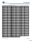
CYV15G0404DXB REFCLKx Switching Characteristics Over the Operating Range
f
REF
REFCLKx Clock Frequency 19.5 150 MHz
t
REFCLK
REFCLKx Period = 1/f
REF
6.6 51.28 ns
t
REFH
REFCLKx HIGH Time (TXRATEx = 1)(Half Rate) 5.9 ns
REFCLKx HIGH Time (TXRATEx = 0)(Full Rate) 2.9
[20]
ns
t
REFL
REFCLKx LOW Time (TXRATEx = 1)(Half Rate) 5.9 ns
REFCLKx LOW Time (TXRATEx = 0)(Full Rate) 2.9
[20]
ns
t
REFD
[25]
REFCLKx Duty Cycle 30 70 %
t
REFR
[20, 21, 22]
REFCLKx Rise Time (20%–80%) 2 ns
t
REFF
[20, 21, 22]
REFCLKx Fall Time (20%–80%) 2 ns
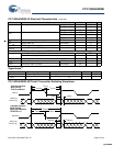
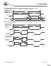
Notes
20.Tested initially and after any design or process changes that may affect these parameters, but not 100% tested.
21.The ratio of rise time to falling time must not vary by greater than 2:1.
22.For a given operating frequency, neither rise or fall specification can be greater than 20% of the clock-cycle period or the data sheet maximum time.
23. Parallel data output specifications are only valid if all outputs are loaded with similar DC and AC loads.
24.Receiver UI (Unit Interval) is calculated as 1/(f
REF
* 20) (when TXRATEx = 1) or 1/(f
REF
* 10) (when TXRATEx = 0). In an operating link this is equivalent to t
B
.
25.The duty cycle specification is a simultaneous condition with the t
REFH
and t
REFL
parameters. This means that at faster character rates the REFCLKx± duty cycle
cannot be as large as 30%–70%.
[+] Feedback [+] Feedback