


Prometheus CPU User Manual V1.44 Page 56
17. GENERATING AN ANALOG OUTPUT
This chapter describes the steps involved in generating an analog output (also called performing
a D/A conversion) on a selected output channel using direct programming (not with the driver
software).
There are three steps involved in performing a D/A conversion:
1. Compute the D/A code for the desired output voltage
2. Write the value to the selected output channel
3. Wait for the D/A to update
17.1 Compute the D/A code for the desired output voltage
Use the formulas on the preceding page to compute the D/A code required to generate the
desired voltage.
⇒ Note: The DAC cannot generate the actual full-scale reference voltage; to do so would require
an output code of 4096, which is not possible with a 12-bit number. The maximum output value is
4095. Therefore the maximum possible output voltage is always 1 LSB less than the full-scale
reference voltage.
17.2 Write the value to the selected output channel
First use the following formulas to compute the LSB and MSB values:
LSB = D/A Code & 255 ;keep only the low 8 bits
MSB = int(D/A code / 256) ;strip off low 8 bits, keep 4 high bits
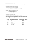
Example:
Output code = 1776
LSB = 1776 & 255 = 240 (F0 Hex); MSB = int(1776 / 256) = int(6.9375) = 6
The LSB is an 8-bit number in the range 0-255. The MSB is a 4-bit number in the range 0-15.
The MSB is always rounded DOWN. The truncated portion is accounted for by the LSB.
Now write these values to the selected channel. The LSB is written to Base + 6. The MSB and
channel number are written to Base + 7. The 2-bit channel no. (0-3) is written to bits 7 and 6, and
the MSB is written to bits 3-0.
outp(Base + 6, LSB);
outp(Base + 7, MSB + channel << 6);
17.3 Wait for the D/A to update
Writing the MSB and channel number to Base + 7 starts the D/A update process for the selected
channel. The update process requires approximately 30 microseconds to transmit the data
serially to the D/A chip and then update the D/A circuit in the chip. During this period, no attempt
should be made to write to any other channel in the D/A through addresses Base + 6 or Base + 7.
The status bit DACBUSY (Base + 3 bit 4) indicates whether the D/A is busy updating (1) or idle
(0). After writing too the D/A, monitor this bit until it is zero before proceeding to the next D/A
operation.