SED1520 Series
2–8 EPSON
level after reset (see Table 1).
When the CS signal is high, the SED1520 series is
disconnected from the MPU bus and set to stand by.
However, the reset signal is entered regardless of the
internal setup status.
BLOCK DESCRIPTION
System Bus
MPU interface
1. Selecting an interface type
The SED1520 series transfers data via 8-bit bidirec-
tional data buses (D0 to D7). As its Reset pin has the
MPU interface select function, the 80-series MPU or
the 68-series MPU can directly be connected to the
MPU bus by the selection of high or low RES signal
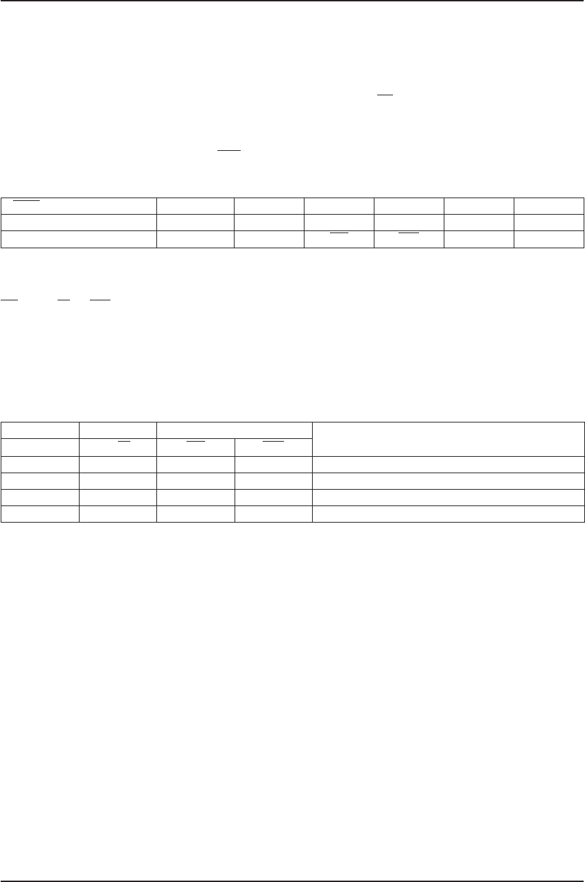
RES signal input level MPU type A0 E R/W CS D0 to D7
Active low 68-series ↑↑↑↑↑
Active high 80-series ↑ RD WR ↑↑
Table 1
Data transfer
The SED1520 and SED1521 drivers use the A0, E (or
RD) and R/W (or WR) signals to transfer data between
the system MPU and internal registers. The combina-
tions used are given in the table blow.
In order to match the timing requirements of the MPU
with those of the display data RAM and control registers
all data is latched into and out of the driver. This
introduces a one cycle delay between a read request for
data and the data arriving. For example when the MPU
executes a read cycle to access display RAM the current
contents of the latch are placed on the system data bus
while the desired contents of the display RAM are moved
into the latch.
This means that a dummy read cycle has to be executed
at the start of every series of reads. See Figure 1.
No dummy cycle is required at the start of a series of
writes as data is transferred automatically from the input
latch to its destination.
Common 68 MPU 80 MPU
Function
A0 R/W RD WR
1 1 0 1 Read display data
1 0 1 0 Write display data
0 1 0 1 Read status
0 0 1 0 Write to internal register (command)


