


SED1520 Series
2–20 EPSON
SPECIFICATIONS
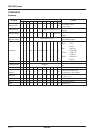
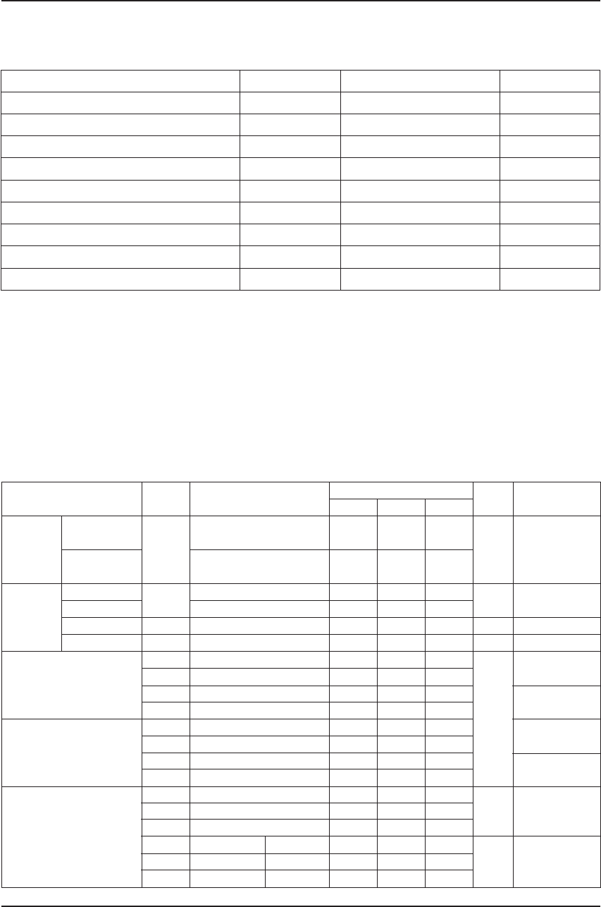
Absolute Maximum Ratings
Parameter Symbol Rating Unit
Supply voltage (1) V
SS –8.0 to +0.3 V
Supply voltage (2) V
5 –16.5 to +0.3 V
Supply voltage (3) V
1, V4, V2, V3 V5 to +0.3 V
Input voltage V
IN VSS–0.3 to +0.3 V
Output voltage V
O VSS–0.3 to +0.3 V
Power dissipation P
D 250 mW
Operating temperature T
opr –40 to +85 deg. C
Storage temperature T
stg –65 to +150 deg. C
Soldering temperature time at lead T
sol 260, 10 deg. C, sec
Notes: 1. All voltages are specified relative to V
DD = 0 V.
2. The following relation must be always hold
V
DD ≥ V1 ≥ V2 ≥ V3 ≥ V4 ≥ V5
3. Exceeding the absolute maximum ratings may cause permanent damage to the device. Functional
operation under these conditions is not implied.
4. Moisture resistance of flat packages can be reduced by the soldering process, so care should be taken to
avoid thermally stressing the package during board assembly.
Electrical Specifications
DC Characteristics
Ta = –20 to 75 deg. C, V
DD = 0 V unless stated otherwise
Rating
Parameter Symbol Condition Unit Applicable Pin
Min. Typ. Max.
Operating Recommended –5.5 –5.0 –4.5
voltage (1) V
SS VVSS
See note 1. Allowable –7.0 — –2.4
Recommended –13.0 — –3.5 V5
V5 V
Operating Allowable –13.0 — — See note 10.
voltage (2) Allowable V1, V2 0.6×V5 —VDD VV1, V2
Allowable V3, V4 V5 — 0.4×V5 VV3, V4
VIHT VSS+2.0 — VDD
See note 2 & 3.
V
IHC 0.2×VSS —VDD
High-level input voltage
V
IHT VSS = –3 V 0.2×VSS —VDD
See note 2 & 3.
V
IHC VSS = –3 V 0.2×VSS —VDD
V
V
ILT VSS VSS+0.8
See note 2 & 3.
V
ILC VSS 0.8×VSS
Low-level input voltage
V
ILT VSS = –3 V VSS 0.85×VSS
See note 2 & 3.
V
ILC VSS = –3 V VSS 0.8×VSS
VOHT IOH = –3.0 mA VSS+2.4 — —
OSC2
V
OHC1 IOH = –2.0 mA VSS+2.4 — — V
See note 4 & 5.
V
OHC2 IOH = –120 µA 0.2×VSS ——
High-level output voltage
V
OHT VSS = –3 V IOH = –2 mA 0.2×VSS
See note 4 & 5.
V
OHC1 VSS = –3 V IOH = –2 mA 0.2×VSS V
OSC2
V
OHC2 VSS = –3 V IOH = –50 µA 0.2×VSS
(continued)