SED1520 Series
EPSON 2–17
SED1520
Series
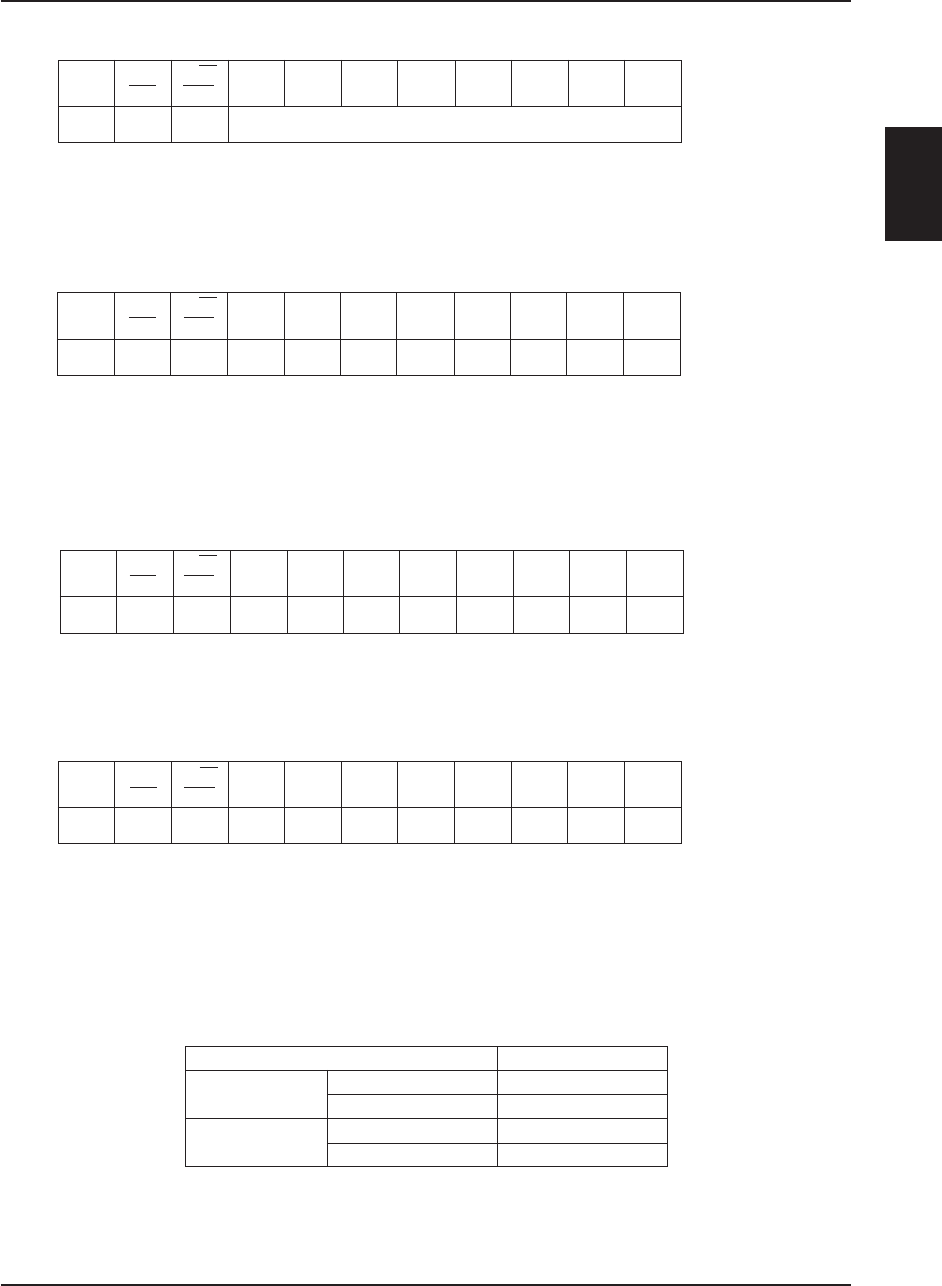
Read Display Data
Reads 8-bits of data from the data I/O latch, updates the contents of the I/O latch with display data from the display data
RAM location specified by the contents of the column address and page address registers and then increments the column
address register.
After loading a new address into the column address register one dummy read is required before valid data is obtained.
Select ADC
This command selects the relationship between display data RAM column addresses and segment drivers.
D=1: SEG0 ← column address 4FH, … (inverted)
D=0: SEG0 ← column address 00H, … (normal)
This command is provided to reduce restrictions on the placement of driver ICs and routing of traces during printed circuit
board design. See Figure 2 for a table of segments and column addresses for the two values of D.
Static Drive ON/OFF
Forces display on and all common outputs to be selected.
D=1: Static drive on
D=0: Static drive off
Select Duty
This command sets the duty cycle of the LCD drive and is only valid for the SED1520F and SED1522F. It is invalid for
the SED1521F which performs passive operation. The duty cycle of the SED1521F is determined by the externally
generated FR signal.
SED1520 SED1522
D=1: 1/32 duty cycle 1/16 duty cycle
D=0: 1/16 duty cycle 1/8 duty cycle
When using the SED1520F
0A, SED1522F0A (having a built-in oscillator) and the SED1521F0A continuously, set the duty
as follows:
R/W
A
0 RD WR D7 D6 D5 D4 D3 D2 D1 D0
1 0 1 Read data
R/W
A
0 RD WR D7 D6 D5 D4 D3 D2 D1 D0
0101010000DA0H, A1H
R/W
A
0 RD WR D7 D6 D5 D4 D3 D2 D1 D0
0101010010DA4H, A5H
R/W
A
0 RD WR D7 D6 D5 D4 D3 D2 D1 D0
0101010100DA8H, A9H
SED1521F0A
SED1520F0A 1/32 1/32
1/16 1/16
SED1522F
0A 1/16 1/32
1/8 1/16


