


APPLICATION NOTE AN42
5
Over-Voltage Protection
The RC5040 and RC5042 constantly monitor the output
voltage for protection against over voltage. If the voltage at
the VFB pin exceeds 20% of the selected program voltage,
an over-voltage condition is assumed, and the controller dis-
ables the output drive signal to the external MOSFET(s).
Short Circuit Protection
A current sense methodology is implemented to disable the
output drive signal to the MOSFET(s) when an over-current
condition is detected. The voltage drop created by the output
current flowing across a sense resistor is presented to an
internal comparator. When the voltage developed across the
sense resistor exceeds the comparator threshold voltage,
the controller disables the output drive signal to the
MOSFET(s).
The DC-DC converter returns to normal operation after the
fault has been removed, for either an over voltage or a short
circuit condition.
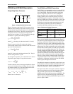
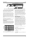
Oscillator
The RC5040 oscillator section is implemented using a
fixed current capacitor charging configuration. An external
capacitor (CEXT) is used to preset the oscillator frequency
between 200KHz and 1MHz. This allows maximum flexibil-
ity in setting the switching frequency and in choosing exter-
nal components.
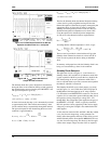
In general, a lower operating frequency increases the peak
ripple current flowing through the output inductor, allowing
the use of a larger inductor value. Operation at lower fre-
quencies increases the amount of energy storage that the
bulk output capacitors must provide during load transients
that occur due to the slower loop response of the controller.
In addition, note that the efficiency losses due to switching
are relatively fixed per switching cycle. Therefore, as the
switching frequency increases, the contribution toward effi-
ciency due to switching losses also increases.
RC5040 has an optimal operating frequency of 650KHz.
This frequency allows the use of smaller inductive and
capacitive components while optimizing peak efficiency
under all operating conditions.
Design Considerations and
Component Selection
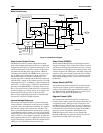
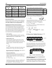
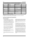
Application Circuits
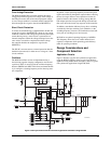
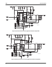
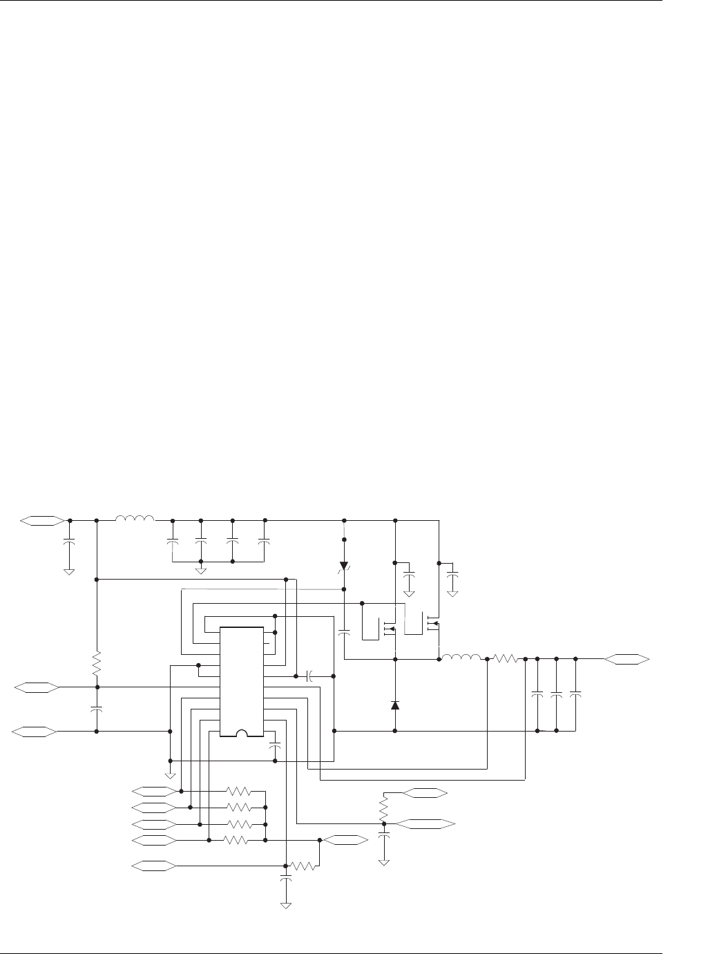
Figure 3 illustrates a typical non-synchronous application
using the RC5040. Figure 4 shows a typical synchronous
application using the RC5040, and Figure 5 shows a typical
non-synchronous application using the RC5042.
Figure 3. Non-Synchronous DC-DC Converter Application Schematic Using RC5040
VO
GND
VID3
VID2
VID1
VID0
8
7
6
5
4
3
2
1
9
1011
12
13
14
15
16
17
18
19
20
VCC
PWRGD
RC5040
VCC
VCC
OUTEN
R5
10K
C10
0.1µF
C11
0.22µF
R6
10K
R4
10K
10K
10K
10K
R3
R2
R1
C
EXT
39pF
C7
0.1µF
C6
4.7µF
DS1
65-AP42-03
MBR1545CT
R7
10K
C1
1000µF
C2
C3
1000µF
1000µF
C5
0.1µF
DS2
1N5817
C12
1µF
L1
1.3µH
M1
2SK1388
M2
2SK1388
C8
C9
0.1µF
0.1µF
R
SENSE
8mΩ
C13
L2
2.6µH
VREF
C14
C15
1500
µ
F
1500
µ
F
C4
0.1µF
1500µF