


APPLICATION NOTE AN42
7
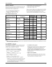
MOSFET Selection
This application requires the use of N-channel, Logic Level
Enhancement Mode Field Effect Transistors. The desired
characteristics of these components are:
• Low Static Drain-Source On-Resistance
R
DS,ON
< 37 mΩ (lower is better)
• Low gate drive voltage, V
GS
≤ 4.5V
• Power package with low thermal resistance
• Drain current rating of 20A minimum
• Drain-Source voltage > 15V.
The on-resistance (R
DS,ON
) is the main parameter for MOS-
FET selection. It determines the MOSFET’s power dissipa-
tion, thus significantly affecting the efficiency of the
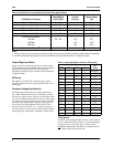
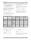
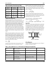
converter. Several suitable MOSFETs are shown in Table 5.
Note:
1. R
DS(ON
) values at Tj = 125°C for most devices were extrapolated from the typical operating curves supplied by the manufac-
turers and are approximations only.
Table 5. MOSFET Selection Table
Manufacturer & Model # Conditions
1
R
DS, ON
(mΩ)
P ackage
Thermal
ResistanceTyp. Max.
Fuji
2SK1388
V
GS
= 4V
I
D
= 17.5A
T
J
= 25°C 25 37 TO-220 Φ
JA
= 75
T
J
= 125°C 37 —
Siliconix
SI4410DY
V
GS
= 4.5V
I
D
= 5A
T
J
= 25°C 16.5 20 SO-8
(SMD)
Φ
JA
= 50
T
J
= 125°C 28 34
National Semiconductor
NDP706AL
V
GS
= 5V
I
D
= 40A
T
J
= 25°C 13 15 TO-220 Φ
JA
= 62.5
Φ
JC
= 1.5
NDP706AEL T
J
= 125°C 20 24
National Semiconductor V
GS
= 4.5V
I
D
= 10A
T
J
= 25°C 31 40 TO-220 Φ
JA
= 62.5
NDP603AL T
J
= 125°C 42 54 Φ
JC
= 2.5
National Semiconductor V
GS
= 5V
I
D
= 24A
T
J
= 25°C 22 25 TO-220 Φ
JA
= 62.5
NDP606AL T
J
= 125°C 33 40 Φ
JC
= 1.5
Motorola V
GS
= 5V
I
D
= 37.5A
T
J
= 25°C 6 9 TO-263 Φ
JA
= 62.5
MTB75N03HDL T
J
= 125°C 9.3 14 (D
2
PAK) Φ
JC
= 1.0
Int. Rectifier V
GS
= 5V
I
D
= 31A
T
J
= 25°C — 28 TO-220 Φ
JA
= 62.5
IRLZ44 T
J
= 125°C — 46 Φ
JC
= 1.0
Int. Rectifier V
GS
= 4.5V
I
D
= 28A
T
J
= 25°C — 19 TO-220 Φ
JA
= 62.5
IRL3103S T
J
= 125°C 31 Φ
JC
= 1.0
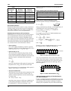
Two MOSFETs in Parallel
We recommend two MOSFETs used in parallel instead of a
single MOSFET. The following significant advantages are
realized using two MOSFETs in parallel:
• Significant reduction of power dissipation.
Maximum current of 14A with one MOSFET:
P
MOSFET
= (I
2
R
DS,ON
)(Duty Cycle) =
(14)
2
(0.050*)(3.3+0.4)/(5+0.4-0.35) = 7.2 W
With two MOSFETs in parallel:
P
MOSFET
= (I
2
R
DS,ON
)(Duty Cycle) =
(14/2)
2
(0.037*)(3.3+0.4)/(5+0.4-0.35) = 1.3W/FET
* Note: R
DS,ON
increases with temperature. Assume R
DS,ON
= 25mΩ
at 25°C. R
DS,ON
can easily increase to 50mΩ at high temperature
when using a single MOSFET. When using two MOSFETs in
parallel, the temperature effects should not cause the R
DS,ON
to rise
above the listed maximum value of 37mΩ.
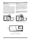
• No added heat sink required.
With the power dissipation down to around one watt and
with MOSFETs mounted flat on the motherboard, no
external heat sink is required. The junction-to-case
thermal resistance for the MOSFET package (TO-220) is
typically at 2°C/W and the motherboard serves as an
excellent heat sink.
• Higher current capability.
With thermal management under control, this on-board
DC-DC converter can deliver load currents up to 14.5A
with no performance or reliability concerns.