


4 - 6 C156-E142-02EN
4.3.1.1 Alternate Status register
This register contains the same information as that of the ATAPI Status register, except that the
ODD does not recognize interrupts when reading this register. Therefore, the ODD does not clear
the INTRQ signal and does not clear interrupts during the pending.
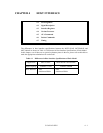
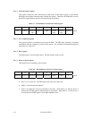
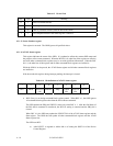
Table 4.5 Bit definitions of Alternate Status register
76543210
BSY DRDY Reserved
(0b)
SERVICE DRQ CORR
(0b)
Reserved
(0b)
CHECK Read
4.3.1.2 ATA Command register
This register contains a command to be passed to the ODD. The ODD starts executing a command
immediately after the command is written in this register. For executable commands and required
parameters, see Table 4.39.
4.3.1.3 Data register
The data register is used for data transfer. The data width is always 16 bits.
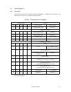
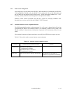
4.3.1.4 Device Control register
This register's bits are defined as shown below.
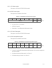
Table 4.6 Bit definitions of Device Control register
76543210
Reserved Reserved Reserved Reserved Reserved SRST nIEN 0 Write
! Bits 7 to 3 are reserved. The ODD ignores all value sets in these bits.
! SRST is a reset bit for host software.
! nIEN is an enable bit for device interrupts to the host. When nIEN is 0 and the device is
selected, the INTRQ signal is enabled by the tri-state buffer. When nIEN is 1 or the device is
not selected, the INTRQ signal is in the high-impedance state.