


111
CHAPTER 8 CLOCK OUTPUT CONTROL CIRCUIT
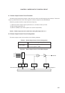
CLOE
PCL/P35 Pin Output
**
CHAPTER 8 CLOCK OUTPUT CONTROL CIRCUIT
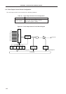
8.1 Clock Output Control Circuit Functions
The clock output control circuit is intended for carrier output during remote controlled transmission and clock output
for supply to peripheral LSI. Clocks selected with the timer clock select register 0 (TCL0) are output from the PCL/
P35 pin.
Follow the procedure below to output clock pulses.
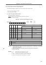
(1) Select the clock pulse output frequency (with clock pulse output disabled) with bits 0 to 3 (TCL00 to TCL03)
of TCL0.
(2) Set the P35 output latch to 0.
(3) Set bit 5 (PM35) of port mode register 3 to 0 (set to output mode).
(4) Set bit 7 (CLOE) of timer clock select register 0 to 1.
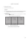
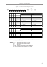
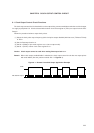
Caution Clock output cannot be used when setting P35 output latch to 1.
Remark When clock output enable/disable is switched, the clock output control circuit does not output pulses
with small widths (See the portions marked with * in Figure 8-1).
Figure 8-1. Remote Controlled Output Application Example