


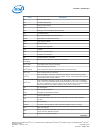
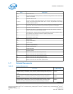
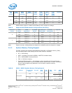
Raw
Card
Version
DIMM
Capacity
DRAM
Device
Technology
DRAM
Organization
# of
DRAM
Devices
# of
Physical
Devices
Ranks
# of
Row / Col
Address
Bits
# of
Banks
Inside
DRAM
Page Size
B
2 GB 1 Gb 128 M X 8 16 2 14/10 8 8K
4 GB 2 Gb 256 M X 8 16 2 15/10 8 8K
4 GB 4 Gb 512 M X 8 8 1 15/10 8 8K
8 GB 4 Gb 512 M X 8 16 2 16/10 8 8K
Note: DIMM module support is based on availability and is subject to change.
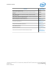
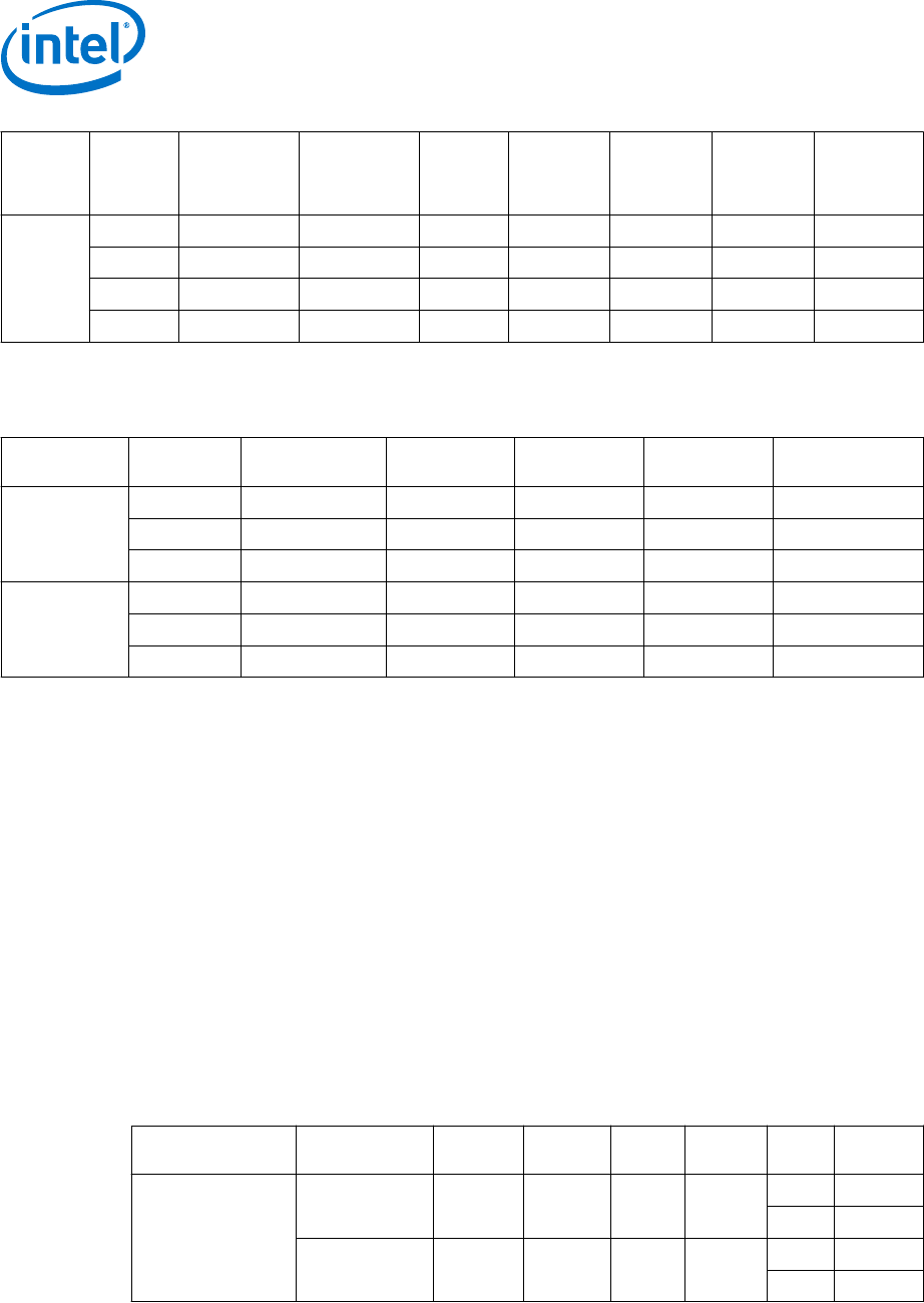
Table 5. Supported SO-DIMM Module Configurations (AIO Only)
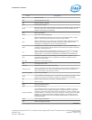
Raw Card
Version
DIMM
Capacity
DRAM
Organization
# of DRAM
Devices
# of Row/Col
Address Bits
# of Banks
Inside DRAM
Page Size
B
1 GB 128 M x 8 8 14/10 8 8K
2 GB 256 M x 8 8 15/10 8 8K
4 GB 512 M x 8 8 16/10 8 8K
F
2 GB 128 M x 8 16 14/10 8 8K
4 GB 256 M x 8 16 15/10 8 8K
8 GB 512 M x 8 16 16/10 8 8K
Note: System memory configurations are based on availability and are subject to change.
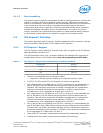
System Memory Timing Support
The IMC supports the following DDR3/DDR3L Speed Bin, CAS Write Latency (CWL),
and command signal mode timings on the main memory interface:
• tCL = CAS Latency
• tRCD = Activate Command to READ or WRITE Command delay
• tRP = PRECHARGE Command Period
• CWL = CAS Write Latency
• Command Signal modes = 1N indicates a new command may be issued every
clock and 2N indicates a new command may be issued every 2 clocks. Command
launch mode programming depends on the transfer rate and memory
configuration.
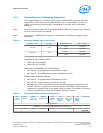
Table 6. DDR3 / DDR3L System Memory Timing Support
Segment Transfer Rate
(MT/s)
tCL (tCK) tRCD
(tCK)
tRP
(tCK)
CWL
(tCK)
DPC CMD
Mode
All segments
1333 8/9 8/9 8/9 7
1 1N/2N
2 2N
1600 10/11 10/11 10/11 8
1 1N/2N
2 2N
2.1.2
Processor—Interfaces
Desktop 4th Generation Intel
®
Core
™
Processor Family, Desktop Intel
®
Pentium
®
Processor Family, and Desktop Intel
®
Celeron
®
Processor Family
Datasheet – Volume 1 of 2 December 2013
20 Order No.: 328897-004