


6.0 Signal Description
This chapter describes the processor signals. The signals are arranged in functional
groups according to the associated interface or category. The following notations are
used to describe the signal type.
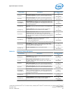
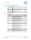
Notation
Signal Type
I Input pin
O Output pin
I/O Bi-directional Input/Output pin
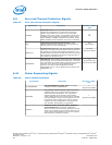
The signal description also includes the type of buffer used for the particular signal
(see the following table).
Table 29. Signal Description Buffer Types
Signal Description
PCI Express*
PCI Express* interface signals. These signals are compatible with PCI Express 3.0
Signaling Environment AC Specifications and are AC coupled. The buffers are not 3.3 V-
tolerant. See the PCI Express Base Specification 3.0.
DMI
Direct Media Interface signals. These signals are compatible with PCI Express 2.0
Signaling Environment AC Specifications, but are DC coupled. The buffers are not 3.3 V-
tolerant.
CMOS CMOS buffers. 1.05V- tolerant
DDR3/DDR3L DDR3/DDR3L buffers: 1.5 V- tolerant
A
Analog reference or output. May be used as a threshold voltage or for buffer
compensation
GTL Gunning Transceiver Logic signaling technology
Ref Voltage reference signal
Asynchronous
1
Signal has no timing relationship with any reference clock.
1. Qualifier for a buffer type.
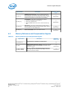
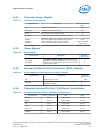
System Memory Interface Signals
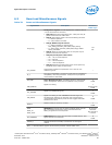
Table 30. Memory Channel A Signals
Signal Name Description Direction / Buffer
Type
SA_BS[2:0]
Bank Select: These signals define which banks are selected
within each SDRAM rank.
O
DDR3/DDR3L
SA_WE#
Write Enable Control Signal: This signal is used with
SA_RAS# and SA_CAS# (along with SA_CS#) to define the
SDRAM Commands.
O
DDR3/DDR3L
continued...
6.1
Processor—Signal Description
Desktop 4th Generation Intel
®
Core
™
Processor Family, Desktop Intel
®
Pentium
®
Processor Family, and Desktop Intel
®
Celeron
®
Processor Family
Datasheet – Volume 1 of 2 December 2013
82 Order No.: 328897-004