


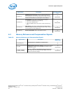
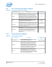
Signal Name Description Direction / Buffer
Type
SB_CK[3:0]
SDRAM Differential Clock: Channel B SDRAM Differential
clock signal pair. The crossing of the positive edge of SB_CK
and the negative edge of its complement SB_CK# are used to
sample the command and control signals on the SDRAM.
O
DDR3/DDR3L
SB_CKE[3:0]
Clock Enable: (1 per rank). These signals are used to:
• Initialize the SDRAMs during power-up.
• Power-down SDRAM ranks.
• Place all SDRAM ranks into and out of self-refresh during
STR.
O
DDR3/DDR3L
SB_CS#[3:0]
Chip Select: (1 per rank). These signals are used to select
particular SDRAM components during the active state. There is
one Chip Select for each SDRAM rank.
O
DDR3/DDR3L
SB_ODT[3:0]
On Die Termination: Active Termination Control. O
DDR3/DDR3L
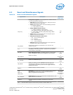
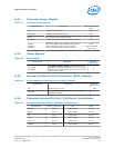
Memory Reference and Compensation Signals
Table 32. Memory Reference and Compensation Signals
Signal Name Description Direction /
Buffer Type
SM_RCOMP[2:0]
System Memory Impedance Compensation: I
A
SM_VREF
DDR3/DDR3L Reference Voltage: This signal is used as
a reference voltage to the DDR3/DDR3L controller and is
defined as V
DDQ
/2
O
DDR3/DDR3L
SA_DIMM_VREFDQ
SB_DIMM_VREFDQ
Memory Channel A/B DIMM DQ Voltage Reference:
The output pins are connected to the DIMMs, and holds
V
DDQ
/2 as reference voltage.
O
DDR3/DDR3L
6.2
Processor—Signal Description
Desktop 4th Generation Intel
®
Core
™
Processor Family, Desktop Intel
®
Pentium
®
Processor Family, and Desktop Intel
®
Celeron
®
Processor Family
Datasheet – Volume 1 of 2 December 2013
84 Order No.: 328897-004