Theory of Operation
316704-001 / Development Kit User’s Manual 27
connector at J5A1. Four ports are routed to USB front panel headers at J6H3 and
J6H4. The last is routed to the PCI-Express* docking connector at J9C1.
There are Five UHCI Host Controllers and two EHCI Host Controllers. Each UHCI Host
Controller includes a root hub with two separate USB ports each, for a total of ten
legacy USB ports. The first EHCI Host Controller includes a root hub that supports up
to six USB 2.0 ports and the second EHCI Host Controller includes a root hub that
supports up to four USB 2.0 ports.
The connection to either the UHCI or EHCI controllers is dynamic and dependant on
the particular USB device. As such, all ports support High Speed, Full Speed, and Low
Speed (HS/FS/LS).
3.4.2.7 LPC Super I/O (SIO)/LPC Slot
An SMSC SIO1007-JV serves as the SIO on the development board. Shunting the
jumper at J7D1 to the 2-3 positions can disable the SIO by holding it in reset. This
allows other SIO solutions to be tested in the LPC slot at J8E1. A sideband header is
provided at J9G1 for this purpose. This sideband header also has signals for LPC
power management. Information on this header is on sheet 44 of the development
board schematics.
3.4.2.8 Serial, IrDA
The SMSC SIO incorporates a serial port, and IrDA (Infrared), as well as general
purpose IOs (GPIO). The Serial Port connector is provided at J2A2, and the IrDA
transceiver is located at U4A1. The IrDA transceiver on the development board
supports SIR (slow IR), FIR (Fast IR) and CIR (Consumer IR). The option to select
between these is supported through software.
3.4.2.9 BIOS Firmware Hub (FWH)
An 8-Mbit Flash device used on the development board to store system and video. The
reference designator location of the FWH device is U8G1. The BIOS can be upgraded
using an MS-DOS* based utility called FWHFlash and is addressable on the LPC bus off
of the ICH8-M. FWHFlash is available on request from your Intel representative.
3.4.2.10 SPI
The Serial Peripheral Interface on ICH8-M is used to support two compatible flash
devices at locations U7E1 and U6D2. By default, the SPI flash is used to store
configuration data for the LAN controller. Optionally it may be used for BIOS and AMT
firmware storage.
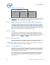
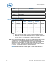
It is necessary to set certain strapping options to enable either a FWH-based or SPI-
based BIOS. Optionally, it is also possible to direct BIOS access to the PCI interface.
Table 7
describes these strapping options.


