


BIOS
Page 4-7
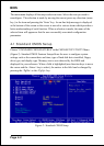
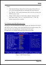
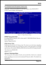
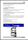
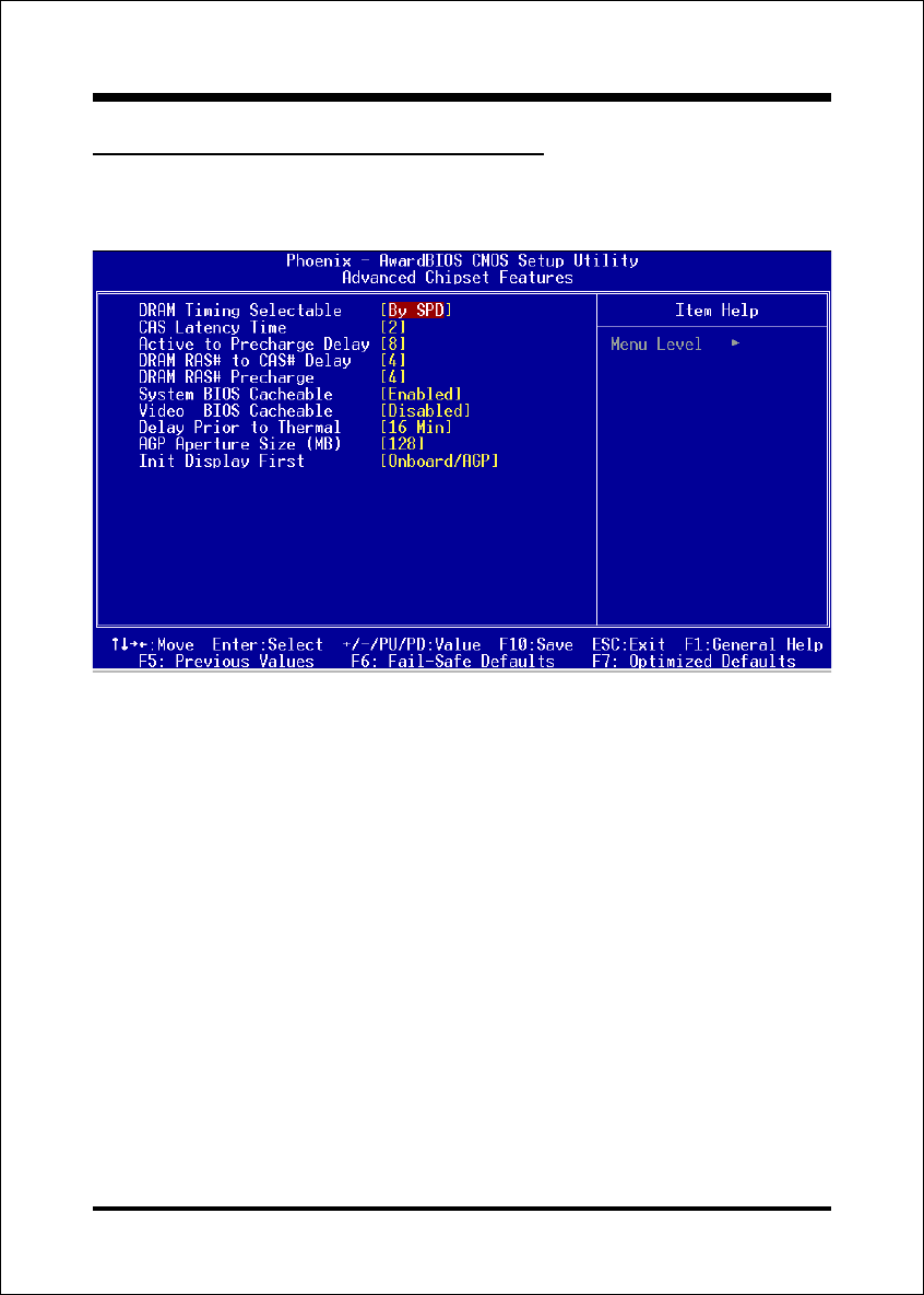
4-3 Advanced Chipset Features
Choose the ADVANCED CHIPSET FEATURES option in the CMOS SETUP
UTILITY menu to display following menu.
Figure 4: Chipset Features Setup
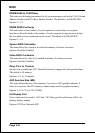
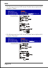
DRAM Timing Selectable
For setting DRAM Timing, By SPD is follow Intel PC DDR SDRAM Serial Presence
Detect Specification.
Options: Manual, By SPD.
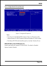
CAS Latency Time
Enables you to select the CAS latency time. The value is set at the factory depending
on the DRAM installed. Do not change the values in this field unless you change
specifications of the installed DRAM and DRAM clock from DRAM Timing Selectable.
The default is by DRAM SPD.
Options: 2, 2.5, 3.
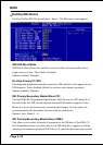
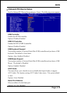
Active to Precharge Delay
This item specifies the number of clock cycles needed after a bank active command
before a precharge can occur (sets the minimum RAS pulse width.). The default is by
DRAM SPD.
Options: 5, 6, 7, 8.