


LXD970A — Demo Board for 10/100 and 100BASE-FX Applications
10 Development Kit Manual
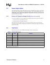
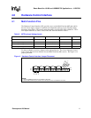
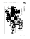
3.0 Jumpers
There are 7 Jumpers on the LXD970 Demo Board. Table 2 describes these jumpers and their
functions.
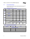
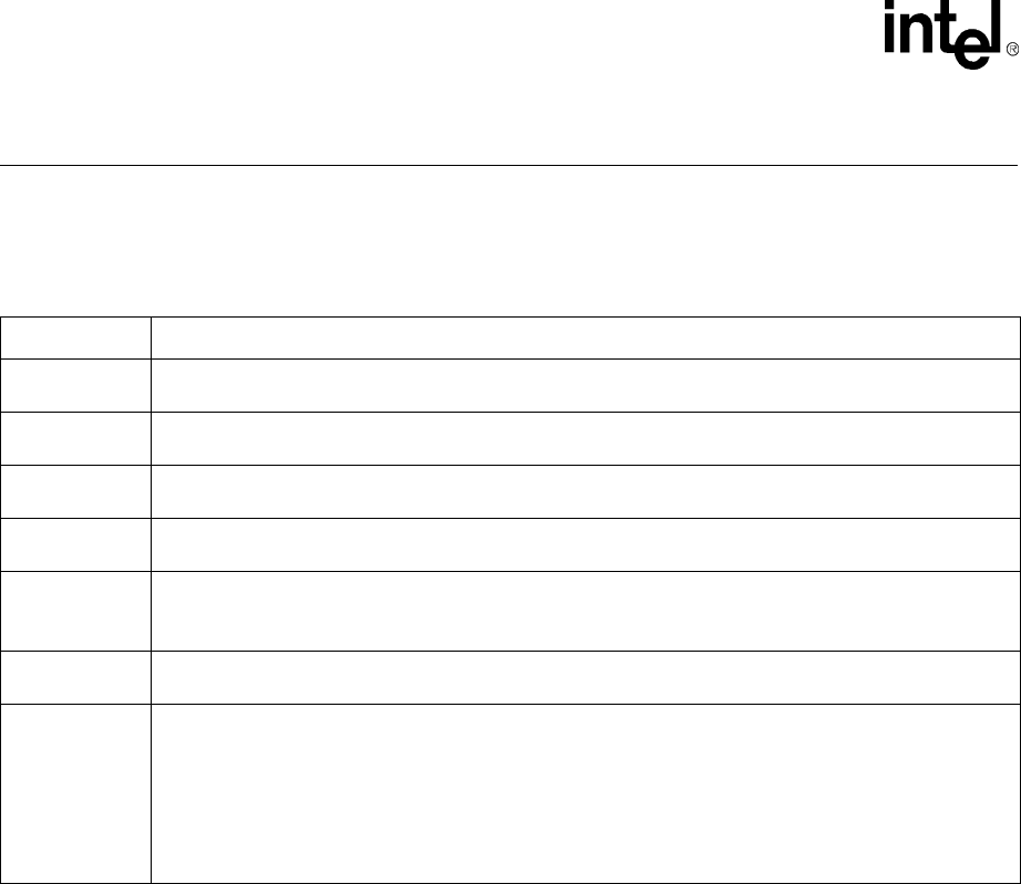
Table 2. Jumper Descriptions
Ref Des Function
JP1
Hardware Control Interface: Provides access to voltage sensitive manual control functions. See Tables 3, 4
and 5 for details.
JP3
MDIO: Connects the MDIO pin to the MII connector. With the trace cut and the jumper open, the MDIO pin
can be connected to an external device.
JP4
MDC: Connects the MDC pin to the MII connector. With the trace cut and the jumper open, the MDC pin can
be connected to an external device.
JP5
TEST: This jumper should not be installed for normal operation. This jumper is used to put the chip into a
test mode that is used to characterize the chip.
JP6
POWER DOWN: With the jumper installed the chip goes into a power down mode.
In power down mode the MII port (except MDIO and MDC), the twisted pair port and the LED pins are
tristated.
JP7
MII: 18-pin straight header that is connected to all the MII interface signal pins. There is a ground test point
next to C20 to ground probes to.
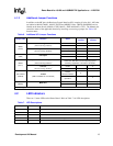
JP8
ANALOG VCC CONNECT: Connects MII connector power to the analog portion of the chip.
To use +5V power from MII connector:
No action required. The jumpers (pins 1 & 2 and 3 & 4) are shorted via a trace on the bottom of board.
However, if the traces are cut, the jumpers must be installed to supply power from MII to analog VCC (VCCA).
To use alternate power supply for Analog VCC:
Cut the trace on the bottom of board across pins 3 and 4 shorting JP8. With no jumpers installed, an external
power can be connected. Provide an alternate power supply ( +5V) to pin 3 of JP8.