


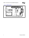

Demo Board for 10/100 and 100BASE-FX Applications — LXD970A
Development Kit Manual 9
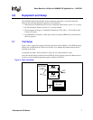
2.3 Power Supply Option
The LXD970A includes a jumper (JP8), which provides a an optional power supply source for the
VCC pins; VCCA (analog supply), VCCR (receive supply), VCCT (transmit supply) and VCCD
(digital supply). In the original factory configuration, this jumper is shorted by a circuit trace and
all LXD970A power is supplied via the MII pin (J1). However, the circuit trace can be easily cut to
provide the JP8 isolation option.
2.3.1 External +5V Supply for Analog Circuitry (VCCA, VCCT and VCCR)
To provide an external +5V power supply for the LXD970A analog circuitry, proceed as follows:
• Cut the circuit trace across JP8 pins 3 and 4
• Attach an external +5V supply to JP8 pin 3
This routes the external supply to VCCA, VCCT, and VCCR (all circuits except VCCD and
VCCIO). To restore to factory configuration, disconnect the external power supply and install the
jumper block in JP8.
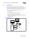
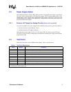
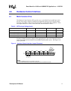
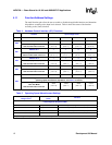
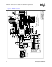
2.4 Test Points
There are 9 Test Points on the LXD970A Demo Board. Table 1 describes these.
Table 1. Test Point Descriptions
Label Ref Des Description
TD+ J3 Transmit Data Output Positive - Signals transmitted from LXD970A to TP link.
TD- J4 Transmit Data Output Negative - Signal transmitted from LXD970A to TP link.
RD+ J5 Receive Data Input Positive - Signals received from TP network.
RD- J6 Receive Data Input Negative - Signals received from TP network.
GNDA J8 Analog Ground
TSTON J9 Test Output Negative
1
TSTOP J10 Test Output Positive
1
IBTST J11 IB Test
1
MDINT J12 Management Data Interrupt
2
- Indicates status change.
1. Factory Test Only
2. 4.7k
Ω pull-up to VCC needed if used