


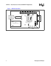
Demo Board for 10/100 and 100BASE-FX Applications — LXD970A
Development Kit Manual 11
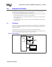
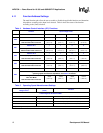
4.0 Hardware Control Interface
4.1 Multi-Function Pins
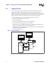
The Hardware Control Interface (JP1) provides access to the Multi-Function (MF) pins which
decode 4-level supply voltages to establish two independent settings per pin. The first setting
determines chip address. The second setting determines configuration of the LXD970A. The 4-
level inputs referred to as V
MF1, VMF2, VMF3 and VMF4 are shown in Table 3.
To select an Input Level place a jumper on the appropriate pins. The 4-level input pins (V
MF1,
VMF2, VMF3 and VMF4) are identical for each Multi-Function (MF) section. See Figure 3 for
jumper placement.
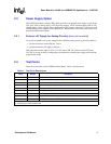
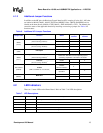
Table 3. MF Pins Input Voltage Levels
Parameter Symbol Min Max Units
Input Voltage Level 1 V
MF1 Vcc - 0.5 - V
Input Voltage Level 2 V
MF2 (Vcc/2) + 0.5 Vcc - 1.2 V
Input Voltage Level 3 V
MF31.2Vcc/2 - 0.5V
Input Voltage Level 4 V
MF4- 0.5V
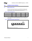
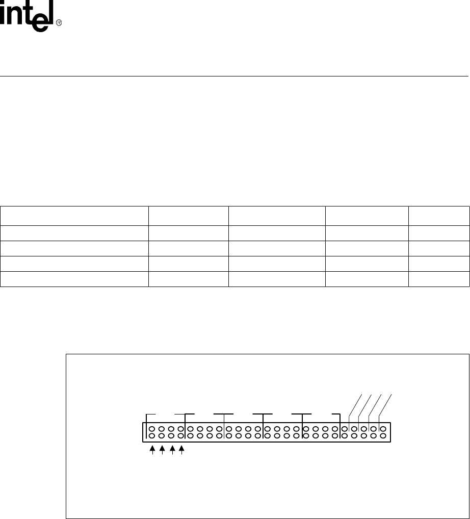
Figure 4. Hardware Control Interface Jumper Placement
NOTES:
1. TRSTE and MDDIS functions are not labeled on the board.
2. CFG1, CFG0 and FDE are pin names for the manual pins and are not labeled on the board.
M
D
D
I
S
1
M
A
N
0
(
C
F
G
0
)
2
M
A
N
1
(
F
D
E
)
2
M
A
N
2
(
C
F
G
1
)
2
T
R
S
T
E
1
pin 49
pin 50
pin 1
pin 2
MF0
MF1 MF2 MF3 MF4
V
MF
1
V
MF
2
V
MF
3
V
MF
4