


Intel
®
LXD972M Transceiver Demo Board (Board Rev A1)
12 Preliminary User’s Guide
Document Number: 303125
Revision Number: 002
Revision Date: October 22, 2004
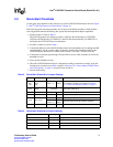
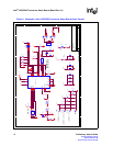
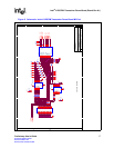
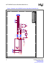
2.4.2 Power Supply Voltage Source and Clock Options
Table 4 lists banana lead power connectors (BNn) for the LXD972M Demo Board. For details on
the power supplies, see the schematic in Chapter 3.0, “Intel
®
LXD972M Demo Board
Schematics”.
Table 5 lists internal and external jumper settings to configure the power supply source for the
transmit magnetic center-tap voltage.
Table 6 lists the LXT972M Demo Board analog power supply (VCCA) configuration options.
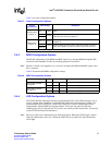
Table 4. Power Supply Voltage Source Connector Options
Reference
Designators
Signal Supply Description
BN1 VCC
+3.3V.
For components on the LXD972M Demo Board other than LXT972M Transceiver.
BN2 GND Ground
BN3 VCCIO
+3.3V or +2.5V.
I/O voltage for the LXT972M Transceiver.
BN4 VCCD
+3.3V.
LXT972M digital power. If JP12 jumper is on, analog power is provided for the
LXT972M Transceiver.
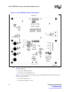
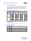
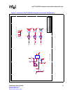
Table 5. Magnetic Center-Tap Voltage Source Configuration Options
Desired
Power Supply Source
Setting Description
3.3V Power Supply from
VCCA
J ump er
JP4
Use Jumper JP4 to apply 3.3V power from VCCA for center-tap
operation.
Alternate Power Supply
Op e n
JP4
Use Jumper JP4 to supply either 2.5V or 3.3V power supply for
center-tap operation. Connect the power supply to pin 2 of JP4.
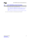
Table 6. Analog Power Supply (VCCA) Configuration Options
Desired
Configuration
Setting Description
Analog
3.3V Power
Supply to VCCA
Jumper
JP12
Use Jumper JP12 to route power from the VCCD Power Connector
(BN4) through JP12 to the VCCA input of the LXT972M Transceiver.
External Power
Supply to VCCA
Open
JP12
1. Remove jumper from JP12 to disable for VCCA input.
2. Apply external power from an alternate power supply through
pin 2 of JP12. For power supply requirements, see the LXT972M
Transceiver datasheet.