


Preliminary User’s Guide 3
Document Number: 303125
Revision Number: 002
Revision Date: October 22, 2004
Contents
Contents
1.0 Introduction......................................................................................................................................5
1.1 About this Demo Board Kit ...................................................................................................5
1.2 Related Documents .............................................................................................................. 5
1.3 Features of Intel
®
LXD972M Demo Board............................................................................6
2.0 Using the Intel
®
LXD972M Demo Board .........................................................................................7
2.1 Equipment Requirements .....................................................................................................7
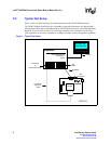
2.2 Typical Test Setup ................................................................................................................8
2.3 Quick-Start Checklists ..........................................................................................................9
2.4 Configurations.....................................................................................................................11
2.4.1 Optional Test Setup, Using Two Intel
®
LXD972M Demo Boards ..........................11
2.4.2 Power Supply Voltage Source and Clock Options.................................................12
2.4.3 MDIO Configuration Options..................................................................................13
2.4.4 LED Configuration Options ....................................................................................13
2.4.5 CFG Pin Configuration Options .............................................................................14
2.5 JTAG Test Signals..............................................................................................................14
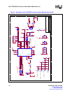
3.0 Intel
®
LXD972M Demo Board Schematics....................................................................................15
4.0 Bill of Materials ..............................................................................................................................20
Figures
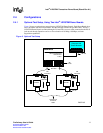
1 Typical Test Setup .......................................................................................................................8
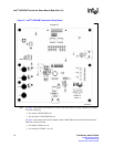
2Intel
®
LXD972M Transceiver Demo Board ................................................................................10
3 Optional Test Setup ...................................................................................................................11
4 Schematic: Intel
®
LXD972M Transceiver Demo Board Power Control ......................................16
5 Schematic: Intel
®
LXD972M Transceiver Demo Board MII Port.................................................17
6 Schematic: Intel
®
LXD972M Transceiver Demo Board Twisted-Pair Port..................................18
7 Schematic: Intel
®
LXD972M Transceiver Demo Board Configuration........................................19
Tables
1 Related Documents ......................................................................................................................5
2 Quick-Start Checklist for Jumper Settings....................................................................................9
3 Quick-Start Checklist for Switch Settings .....................................................................................9
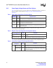
4 Power Supply Voltage Source Connector Options .....................................................................12
5 Magnetic Center-Tap Voltage Source Configuration Options.....................................................12
6 Analog Power Supply (VCCA) Configuration Options ................................................................12
7 Clock Configuration Options.......................................................................................................13
8 MDIO Configuration Options.......................................................................................................13
9 Jumper Configuration Settings for LED/CFG Pins......................................................................14
10 JTAG Test Signal Descriptions...................................................................................................14
11 Bill of Materials ...........................................................................................................................20