


Intel
®
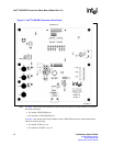
LXD972M Transceiver Demo Board (Board Rev A1)
14 Preliminary User’s Guide
Document Number: 303125
Revision Number: 002
Revision Date: October 22, 2004
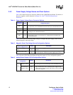
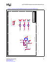
2.4.5 CFG Pin Configuration Options
Three control jumpers pull the associated port configuration pins High or Low to select the desired
mode (auto-negotiation, speed, and duplex). When auto-negotiation is enabled with LED/CFG1
(JP1) = 1, then LED/CFG2 (JP2), and LED/CFG3 (JP3) are used to configure default advertising
characteristics of the LXD972M Demo Board. The desired modes and jumper configuration
settings are listed in Table 9. For specific register definitions and functions, see the LXT972M
Transceiver datasheet.
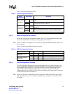
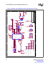
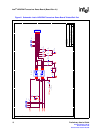
2.5 JTAG Test Signals
The boundary scan test port is accessed through JP14 for board level testing. Table 10 lists the
JTAG test signal descriptions.
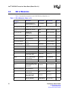
Table 9. Jumper Configuration Settings for LED/CFG Pins
Mode Jumper Settings
Auto-
Negotiation
Speed Duplex
JP1
LED/CFG1
Setting
JP2
LED/CFG2
Setting
JP3
LED/CFG3
Setting
Disabled
10
Half
Jumper
Pins 2 & 3
Jumper
Pins 2 & 3
Jumper
Pins 2 & 3
Full Pins 2 & 3 Pins 2 & 3 Pins 1 & 2
100
Half Pins 2 & 3 Pins 1 & 2 Pins 2 & 3
Full Pins 2 & 3 Pins 1 & 2 Pins 1 & 2
Enabled
100
Half Pins 1 & 2 Pins 2 & 3 Pins 2 & 3
Full /
Half
Pins 1 & 2 Pins 2 & 3 Pins 1 & 2
10/100
Half Pins 1 & 2 Pins 1 & 2 Pins 2 & 3
Full /
Half
Pins 1 & 2 Pins 1 & 2 Pins 1 & 2
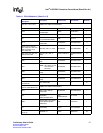
Table 10. JTAG Test Signal Descriptions
JP14 Pin
Number
Symbol Description
1TRST_LTest Reset. Test reset input sourced by testing device.
3TCK
Test Clock. Test clock input sourced by testing device.
5TMS
Test Mode Select.
7TDO
Test Data Output. Test data driven with respect to the falling edge of TCK.
8TDI
Test Data Input. Test data sampled with respect to the rising edge of TCK.