


User’s Manual 147
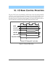
The eight I/O bank control registers determine the number of I/O wait states applied to an
external I/O access within the zone controlled by each register even if the associated
strobes are not enabled. Note that the /IORD and /IOWR signals reflect these registers as
well.
The control over the generation of wait states is independent of whether or not the associ-
ated strobe in Port E is enabled. The upper 2 bits of each register determine the number of
wait states. The four choices are 1, 3, 7, or 15 wait states. On reset, the bits are cleared,
resulting in 15 wait states. There is always at least one external I/O wait state, and thus the
minimum external I/O read cycle is three clocks long. The inhibit write function applies to
both the Port E write strobes and the /IOWR signal.
These control bits have no effect on the internal I/O space, which does not have wait states
associated with read or write access. Internal I/O read or write cycles are two clocks long.
The I/O strobes greatly simplify the interfacing of external devices. On reset, the upper 5
bits of each register are cleared. Parallel Port E will not output these signals unless the
data-direction register bits are set for the desired output positions. In addition, the Port E
function register must be set to "1" for each position.
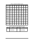
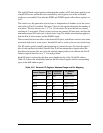
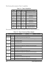
Each I/O bank is selected by the three most significant bits of the 16-bit I/O address.
Table 10-2 shows the relationship between the I/O control register and its corresponding
space in the 64K address space.
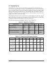
Table 10-2. External I/O Register Address Range and Pin Mapping
Control Register
Port E
Pin
I/O Address
A[15:13]
I/O Address
Range
IB0CR PE0 000 0x0000–0x1FFF
IB1CR PE1 001 0x2000–0x3FFF
IB2CR PE2 010 0x4000–0x5FFF
IB3CR PE3 011 0x6000–0x7FFF
IB4CR PE4 100 0x8000–0x9FFF
IB5CR PE5 101 0xA000–0xBFFF
IB6CR PE6 110 0xC000–0xDFFF
IB7CR PE7 111 0xE000–0xFFFF