


60 Rabbit 3000 Microprocessor
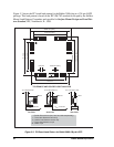
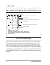
5.2.2 Mechanical Dimensions and Land Pattern
The design considerations in Table 5-3 are based on 5 mil design rules and assume a single
conductor between solder lands.
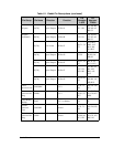
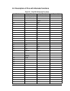
Table 5-2. Ball and Land Size Dimensions
Nominal Ball
Diameter
(mm)
Tolerance
Variation
(mm)
Ball Pitch
(mm)
Nominal Land
Diameter
(mm)
Land
Variation
(mm)
0.3 0.35–0.25 0.8 0.25 0.25–0.20
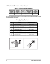
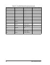
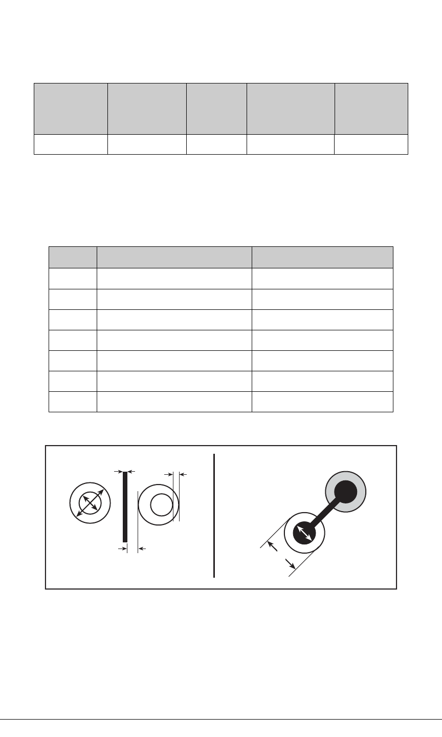
Table 5-3. Design Considerations
(all dimensions in mm)
Key Feature Recommendation
A Solder Land Diameter 0.254 (0.010)
B NSMD Defined Land Diameter 0.406 (0.016)
C Land to Mask Clearance (min.) 0.050 (0.002)
D Conductor Width (max.) 0.127 (0.005)
E Conductor Spacing (typ.) 0.127 (0.005)
F Via Capture Pad (max.) 0.406 (0.016)
G Via Drill Size (max.) 0.254 (0.010)
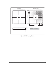
A
B
C
D
E
Land and Trace
Via
G
F