


Chapter 4. BUFFER MEMORY CONFIGURATION AND FUNCTIONS
4- 1
Chapter 4. BUFFER MEMORY CONFIGURATION AND FUNCTIONS
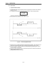
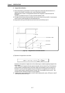
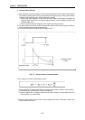
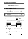
The PID control module has the PLC CPU and the buffer memories for communications.
4.1 Buffer memory Configuration
The followings describe buffer memory configuration.
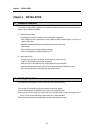
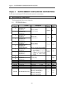
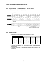
4.1.1 K7F-PIDA Buffer Memory
Address
(Decimal)
Function Descriptions
Default
Setting
Read /
Write
0
Loop enable/disable
Specification area
(loop 0 to 15)
1
Loop enable/disable
Specification area
(loop 16 to 31)
Bit On(1): Enabled
Bit Off(0): Disabled
Disabled R/W
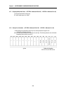
2
Auto/Manual operation
Specification area
(loop 0 to 15)
3
Auto/Manual operation
Specification area
(loop 16 to 31))
Bit On(1): Auto
Bit Off(0): Manual
Auto R/W
4
Forward/Reverse action
Specification area
(loop 0 to 15)
5
Forward/Reverse action
Specification area
(loop 16 to 31)
Bit On(1): Reverse
Bit Off(0): Forward
Forward R/W
6
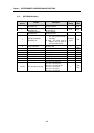
Set data enable/disable
Specification area
(loop 0 to 15)
7
Set data enable/disable
Specification area
(loop 16 to 31)
Bit On(1) : Set each content of address
0, 1, 4, 5, 10 to 41, and 74 to 201
to a new setting.
Bit Off(0) : The previous values of
address 0, 1, 4, 5, 10 to 41, and
74 to 201 remains without
change.
No Setting
Values
R/W
8
Loop run information
(loop 0 to 15)
9
Loop run information
(loop 16 to 31)
Bit On(1) : Run
Bit Off(0) : Stop
Read
Only
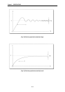
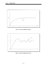
10 to 41 SV of each loop Setting range : 0 to 16000 “0” R/W
42 to 73 PV of each loop Input range : 0 to 16000 “0” R/W
74 to 105 M-MV of each loop Setting range : 0 to 16000 “0” R/W
106 to 137 P of each loop Setting range : 0 to 10000 “500” R/W
138 to 169 I of each loop Setting range : 0 to 30000 “1000” R/W
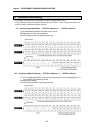
170 to 201 D of each loop Setting range : 0 to 30000 “0” R/W
202 to 233 MV of each loop Output range : 0 to 16000
Read
234 to 265 Error information of each loop
Bit 0 On(1) : out-of-range SV
Bit 1 On(1) : out-of-range PV
Bit 2 On(1) : out-of-range M_MV
Bit 3 On(1) : out-of-range P
Bit 4 On(1) : out-of-range I
Bit 5 On(1) : out-of-range D
Read
Only