


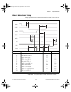
Chapter 4 Signal Connections
©
National Instruments Corporation 4-25 PCI-6023E/6024E/6025E User Manual
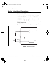
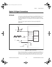
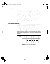
2. Using the following formula, calculate the largest possible load to
maintain a logic low level of 0.4 V and supply the maximum driving
current:
V = I * R
L
⇒ R
L
= V/I, where:
V = 0.4 V ; Voltage across R
L
I = 46 µA + 10 µA ; 4.6 V across the 100 kΩ pull-up resistor
and 10 µA maximum leakage current
Therefore:
R
L
= 7.1 kΩ ; 0.4 V/56 µA
This resistor value, 7.1 kΩ, provides a maximum of 0.4 V on the DIO line
at power up. You can substitute smaller resistor values to lower the voltage
or to provide a margin for V
cc
variations and other factors. However,
smaller values will draw more current, leaving less drive current for other
circuitry connected to this line. The 7.1 kΩ resistor reduces the amount of
logic high source current by 0.4 mA with a 2.8 V output.
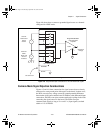
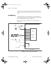
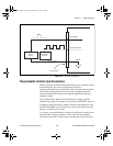
Timing Specifications
♦ (PCI-6025E Only)
This section lists the timing specifications for handshaking with your
PCI-6025E PC<0..7> lines. The handshaking lines STB* and IBF
synchronize input transfers. The handshaking lines OBF* and ACK*
synchronize output transfers. Table 4-4 describes signals appearing in the
handshaking diagrams.
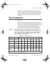
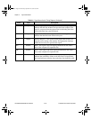
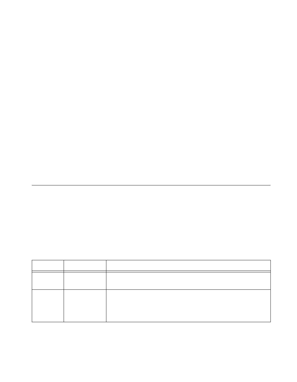
Table 4-4.
Signal Names Used in Timing Diagrams
Name Type Description
STB* Input Strobe Input—A low signal on this handshaking line loads data into
the input latch.
IBF Output Input Buffer Full—A high signal on this handshaking line indicates
that data has been loaded into the input latch. A low signal indicates
the board is ready for more data. This is an input acknowledge
signal.
PCI.book Page 25 Wednesday, September 16, 1998 9:09 AM