


Getting Started with R Series Intelligent DAQ 10 ni.com
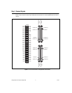
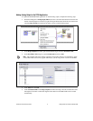
6. Right-click the input terminal of the new FPGA I/O Node and select Create»Control from the
shortcut menu. Rename the control AO Voltage, as shown in the following block diagram.
7. Save the VI, then right-click Analog Input (FPGA).vi in the Project Explorer window and select
Compile from the shortcut menu to recompile the FPGA VI.
8. Modify the host VI to control the additional AO channel you created by completing the
following steps:
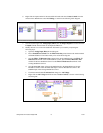
a. Open the Analog Input (Host).vi block diagram.
b. Place a Read/Write Control from the FPGA Interface palette between the Invoke method
and the Read/Write Control that already exists on the block diagram.
c. Wire the FPGA VI Reference Out terminal of the Invoke Method node to the FPGA VI
Reference In terminal of the new Read/Write Control. Wire the FPGA Reference Out
terminal of the new Read/Write Control to the FPGA VI Reference In terminal of the
existing Read/Write Control.
d. Wire the error out output of the Invoke Method node to the error in input of the new
Read/Write Control. Wire the error out output of the new Read/Write Control to the
error in input of the existing Read/Write Control.
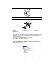
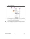
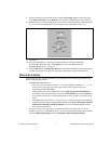
e. Click the terminal labeled Unselected and change it to AO Voltage.
f. Right-click the AO Voltage terminal and select Create»Control, as shown in the following
block diagram.