


1996 Dec 12 17
Philips Semiconductors Product specification
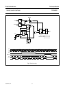
Smart card interface TDA8001
Notes
1. Pins CMDVCC, VPP21, VPP15, VPP12.5, CMD7, CMD3.5 and PRES are active LOW; pins RSTIN and PRES are
active HIGH.
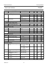
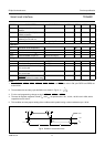
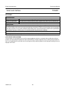
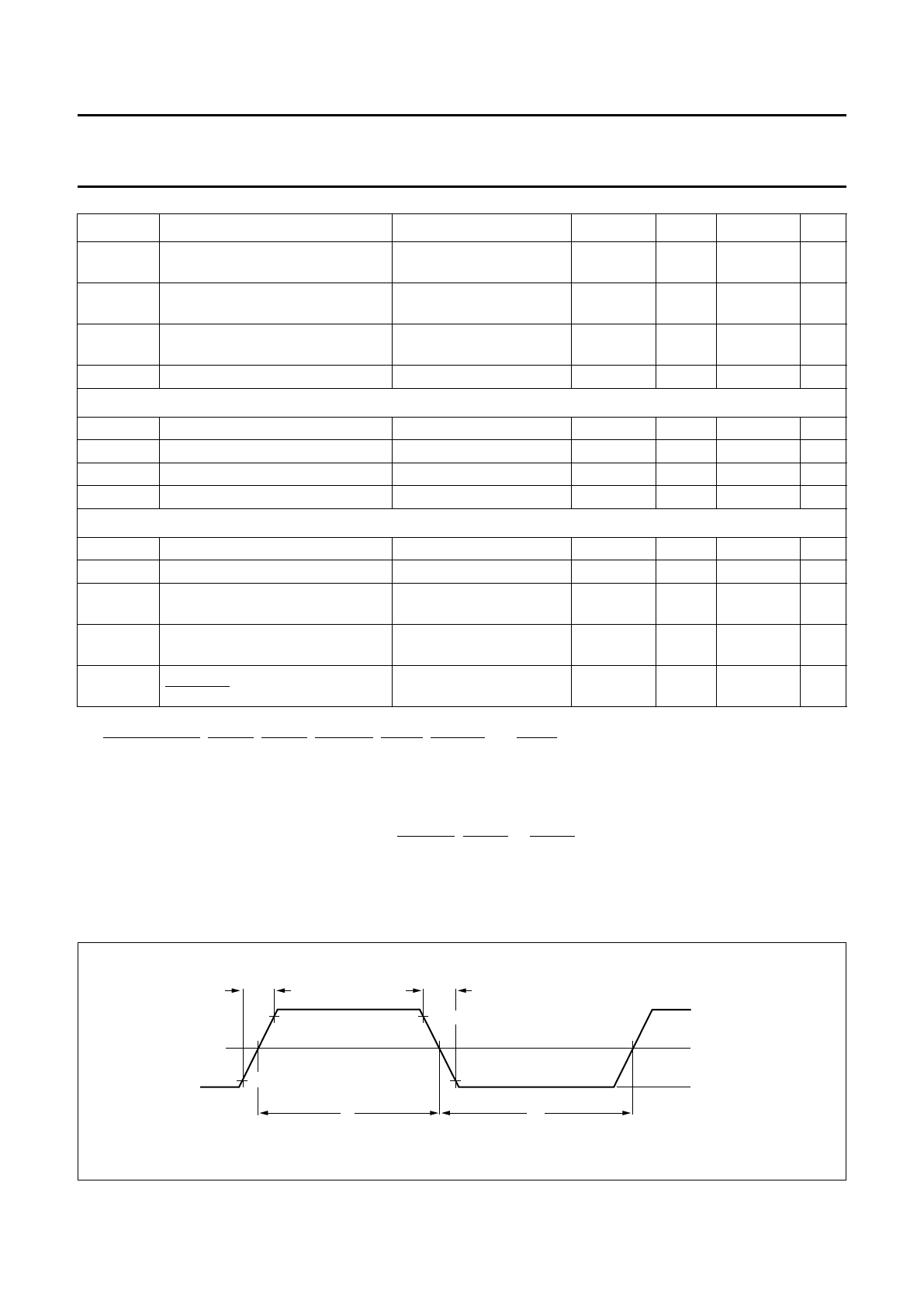
2. The transition time and duty cycle definitions are shown in Fig.12; .
3. P is the card programming voltage set by pin VPP12.5, VPP15 or VPP21.
4. The tests for dynamic response of both V
PP
and V
CC
are performed at 1 Hz, 10 kHz, 100 kHz and 1 MHz, with a
capacitive load of 100 nF.
5. This condition ensures proper starting of the oscillator with crystals having a series resistance up to 100 Ω.
V
IDLE
voltage on pin I/O outside a
session
−−0.4 V
Z
IDLE
impedance on pin I/O(µC)
outside a session
10 −− MΩ
R
pu
internal pull-up resistance
between pin I/O and V
CC
81012kΩ
t
r
, t
f
rise and fall times C
i
=C
o
=30 pF −−0.5 µs
Protections
T
sd
shut-down local temperature − 135 −°C
I
CC(sd)
shut-down current at V
CC
−−150 − mA
I
PP(sd)
shut-down current at V
PP
−−75 − mA
I
I/O(lim)
current limitation on pin I/O from I/O to I/O(µC) 3 − 5mA
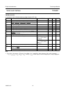
Timing
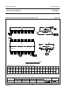
t
act
activation sequence duration see Fig.7 − 110 −µs
t
de
deactivation sequence duration see Fig.8 − 100 −µs
t
3
start of the window for sending
CLK to the card
−−70 µs
t
5
end of the window for sending
CLK to the card
80 −− µs
t
st
maximum pulse width on
CMDVCC before V
CC
starts rising
−−30 µs
SYMBOL PARAMETER CONDITIONS MIN. TYP. MAX. UNIT
δ
t
1
t
1
t
2
+
---------------
=
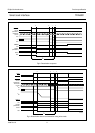
Fig.12 Definition of transition times.
handbook, full pagewidth
MBH856
10%
90%
10%
V
OH
V
OL
1.5 V
90%
t
f
t
r
t
2
t
1