


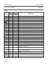

1996 Dec 12 8
Philips Semiconductors Product specification
Smart card interface TDA8001
READ MODE
When the activation sequence is completed and, after the
card has replied its Answer-to-Reset, the TDA8001 will be
in the READ mode. Data is exchanged between the card
and the microcontroller via the I/O line.
W
RITE MODE
Cards with EPROM memory need a programming voltage
(V
PP
). When it is required to write to the internal memory
of the card, the microcontroller sets one of the VPP12.5,
VPP15 and VPP21 lines LOW, according to the
programming value given in the Answer-to-Reset.
V
PP
rises from 5 V to the selected value with a typical slew
rate of 0.38 V/µs. In order to respect the ISO 7816 slopes,
the circuit generates V
PP
by charging and discharging an
internal capacitor. The voltage on this capacitor is then
amplified by a power stage gain of 5, powered via an
external supply pin V
H
(30 V max).
D
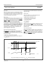
EACTIVATION SEQUENCE (see Fig.8)
When the session is completed, the microcontroller sets
the CMDVCC line to its HIGH state. The circuit then
executes an automatic deactivation sequence by counting
the sequencer back:
• RST falls to LOW and CLK is stopped
• I/O(µC) becomes high impedance and V
PP
falls to 0 V
• V
CC
falls to 0 V.
The circuit returns to the IDLE mode on the next rising
edge of the clock.
P
ROTECTIONS
Main fault conditions are monitored by the circuit:
• Short-circuit or overcurrent on V
CC
• Short-circuit or overcurrent on V
PP
• Card extraction during transaction
• Overheating problem
• V
SUP
drop-out
• V
DD
drop-out.
When one of these fault conditions is detected, the circuit
pulls the interrupt line
OFF to its active LOW state and
returns to the FAULT mode. The current on I/O is internally
limited to 5 mA.
F
AULT MODE (see Fig.9)
When a fault condition is written to the microcontroller via
the OFF line, the circuit initiates a deactivation sequence.
After the deactivation sequence has been completed, the
OFF line is reset to its HIGH state after the microcontroller
has reset the CMDVCC line HIGH.
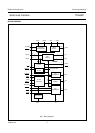
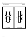
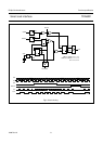
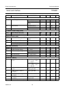
Fig.4 Alarm and delay as a function of V
SUP
(C
DEL
fixes the pulse width).
handbook, full pagewidth
MGG818
V
SUP
V
th2
+ V
hys2
V
th2
V
th3
t
d
V
DELAY
ALARM