


1996 Dec 12 7
Philips Semiconductors Product specification
Smart card interface TDA8001
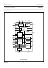
FUNCTIONAL DESCRIPTION
Power supply
The circuit operates within a supply voltage range of
6.7 to 18 V. V
DD
and GND are the supply pins. All card
contacts remain inactive during power up or down.
P
OWER UP
The logic part is powered first and is in the reset condition
until V
DD
reaches V
th1
. The sequencer is blocked until V
DD
reaches V
th4
+V
hys4
.
P
OWER DOWN
When V
DD
falls below V
th4
, an automatic deactivation of
the contacts is performed.
Voltage supervisor
This block surveys the 5 V supply of the microcontroller
(V
SUP
) in order to deliver a defined reset pulse and to avoid
any transients on card contacts during power up or down
of V
SUP
. The voltage supervisor remains active even if V
DD
is powered-down.
P
OWER ON
As long as V
SUP
is below V
th2
+V
hys2
the capacitor C
DEL
,
connected to pin DELAY, will be discharged. When V
SUP
rises to the threshold level, C
DEL
will be recharged.
ALARM and ALARM remain active, and the sequencer is
blocked until the voltage on the DELAY line reaches V
th3
.
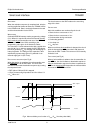
P
OWER DOWN (see Fig.4)
If V
SUP
falls below V
th2
, C
DEL
will be discharged, ALARM
and ALARM become active, and an automatic deactivation
of the contacts is performed.
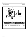
Clock circuitry (see Fig.5)
The clock signal (CLK) can be applied to the card in two
different methods:
1. Generation by a crystal oscillator: the crystal, or the
ceramic resonator (4 to 16 MHz) is connected to the
XTAL pin.
2. Use of a signal frequency (up to 20 MHz), already
present in the system and connected to the XTAL pin
via a 10 nF capacitor (see Fig.14). In both cases the
frequency is first divided-by-two.
If
CMD7 (respectively CMD3.5) is LOW, the clock signal
(its frequency again divided by two) is enabled and
buffered before being fed to the CLK pin.
CMD3.5 and internal ENRST are sampled in order to give
the first clock pulse the correct width, and to avoid false
pulses during frequency change.
The CLKOUT2 pins may be used to clock a
microcontroller or an other TDA8001. The signal
1
⁄
2
f
xtal
is
available when the circuit is powered up.
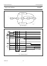
State diagram
Once activated, the circuit has six possible modes of
operation:
• Idle
• Activation
• Read
• Write
• Deactivation
• Fault.
Figure 6 shows the way these modes are accessible.
I
DLE MODE
After reset, the circuit enters the IDLE state. A minimum
number of circuits are active while waiting for the
microcontroller to start a session.
• All card contacts are inactive
• I/O(µC) is high impedance
• Voltage generators are stopped
• Oscillator or XTAL input is running, delivering CLKOUT2
• Voltage supervisors are active.
The DETECT line is HIGH if a card is present (PRES and
PRES active) and LOW if a card is not present. The OFF
line is HIGH if no hardware problem is detected.
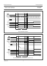
A
CTIVATION SEQUENCE
From the IDLE mode, the circuit enters the ACTIVATION
mode when the microcontroller sets the CMDVCC line
(active LOW). The I/O(µC) signal must not be LOW.
The internal circuitry is activated, the internal clock starts
and the sequence according to ISO7816 is performed:
• V
CC
rises from 0 to 5 V
• V
PP
rises from 0 to 5 V and I/O is enabled
• CLK and RST are enabled.
The time interval between steps 1 and 2 is 16 µs, and
64 µs between steps 2 and 3 (see Fig.7).