


1996 Dec 12 5
Philips Semiconductors Product specification
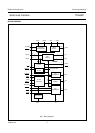
Smart card interface TDA8001
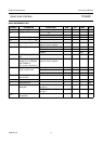
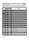
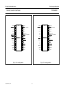
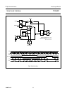
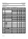
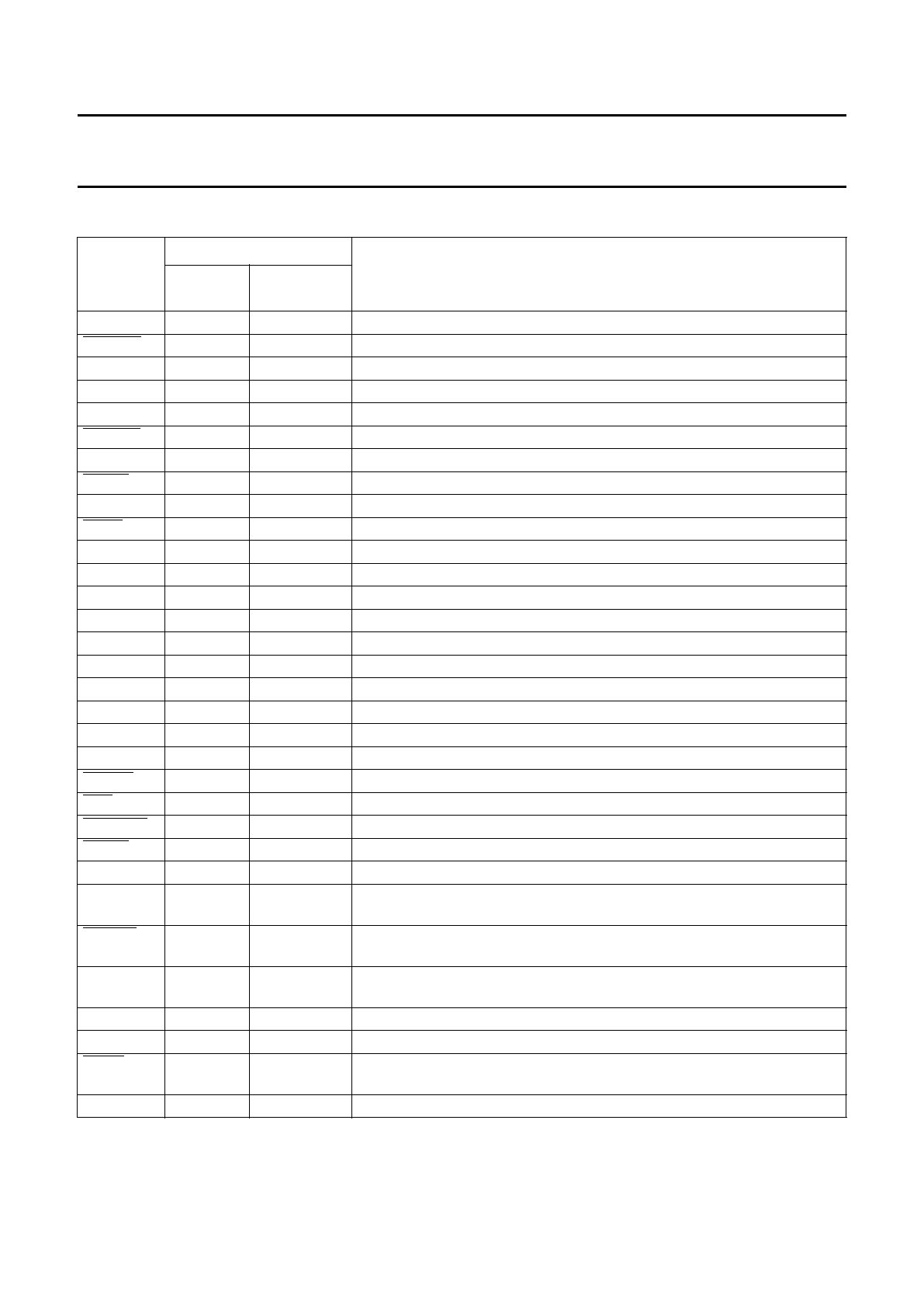
PINNING
SYMBOL
PIN
DESCRIPTION
TDA8001
TDA8001T
TDA8001A
TDA8001AT
XTAL 1 1 crystal connection
DETECT 2 2 card extraction open collector output (active LOW)
I/O 3 3 data line to/from the card
RST 4 4 card reset output
CLK 5 5 clock output to the card
VPP12.5 6 − control input for applying the 12.5 V programming voltage (active LOW)
n.c. − 6 not connected
VPP15 7 − control input for applying the 15 V programming voltage (active LOW)
n.c. − 7 not connected
PRES 8 8 card presence contact input (active LOW)
PRES 9 9 card presence contact input (active HIGH)
V
PP
10 − card programming voltage output
n.c. − 10 not connected
V
H
11 11 HIGH voltage supply for V
PP
generation
GND1 12 12 ground 1
V
DD
13 13 positive supply voltage
V
CC
14 14 card supply output voltage
V
SUP
15 15 voltage supervisor input
DELAY 16 16 external capacitor connection for delayed reset timing
ALARM 17 17 open-collector reset output for the microcontroller (active HIGH)
ALARM 18 18 open-collector reset output for the microcontroller (active LOW)
OFF 19 19 open-collector interrupt output to the microcontroller (active LOW)
CMDVCC 20 20 control input for applying supply voltage to the card (active LOW)
VPP21 21 − control input for applying the 21 V programming voltage (active LOW)
n.c. − 21 not connected
CVNC 22 22 internally generated 5 V reference, present when V
DD
is on; to be
decoupled externally (100 nF)
CMD3.5
or CDMTC
23 23 control input for having the crystal frequency divided-by-4 at pin CLK
CLKOUT2 24 24 clock output to the microcontroller, or any other R4590
(crystal frequency divided by two)
GND2 25 25 ground 2
RSTIN 26 26 card reset input from the microcontroller (active HIGH)
CMD7
or CDMS
27 27 control input for having the crystal frequency divided by 2 at pin CLK
I/O(µC) 28 28 data line to/from the microcontroller