


M306V8T-EPB User’s Manual 4. Hardware Specifications
REJ10J0777-0100 Rev.1.00 2005.08.01 Page 65 of 90
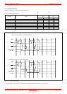
4.2 Access Timing
Because this product emulates some ports, access timings are different from those of the actual MCUs. Chapter 4.2.1 describes
the access timing using this product.
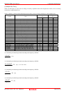
4.2.1 Operation Timing of Memory Expansion Mode and Microprocessor Mode (Vcc1=Vcc2=Vcc3=3.3V)
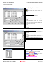
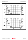
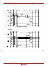
(1) Separate Bus Timing
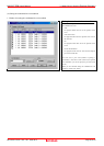
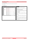
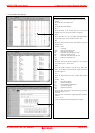
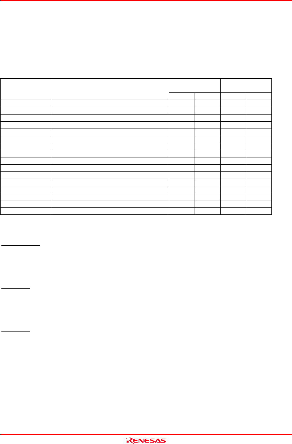
Table 4.2 and Figure 4.1 show the bus timing in memory expansion mode and microprocessor mode.
Table 4.2 Memory expansion mode and microprocessor mode (3-wait, accessing external area)
Actual MCU
[ns]
This product
[ns]
Symbol Item
Min. Max. Min. Max.
td(BCLK-AD) Address output delay time 30 36
th(BCLK-AD) Address output hold time (BCLK standard) 4 See left
th(RD-AD) Address output hold time (RD standard) 0 -3
th(WR-AD) Address output hold time (WR standard) (*2) (*3)
td(BCLK-CS) Chip-select output delay time 30 See left
th(BCLK-CS) Chip-select output hold time (BCLK standard) 4 See left
td(BCLK-ALE) ALE signal output delay time 30 See left
th(BCLK-ALE) ALE signal output hold time -4 See left
td(BCLK-RD) RD signal output delay time 30 33
th(BCLK-RD) RD signal output hold time 0 See left
td(BCLK-WR) WR signal output delay time 30 38
th(BCLK-WR) WR signal output hold time 0 See left
td(BCLK-DB) Data output delay time (BCLK standard) 40 43
th(BCLK-DB) Data output hold time (BCLK standard) 4 See left
td(DB-WR) Data output delay time (WR standard) (*1) See left
th(WR-DB) Data output hold time (WR standard) (*2) (*3)
*1 Calculated by the following formula according to the frequency of BCLK.
()
40
)(
105.0
9
−
×−
BCLKf
n
[ns] n: "3" for 3-wait
*2 Calculated by the following formula according to the frequency of BCLK.
)(
105.0
9
BCLKf
×
[ns]
*3 Calculated by the following formula according to the frequency of BCLK.
17
)(
105.0
9
−
×
BCLKf
[ns]