


M306V8T-EPB User’s Manual 4. Hardware Specifications
REJ10J0777-0100 Rev.1.00 2005.08.01 Page 73 of 90
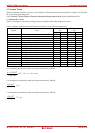
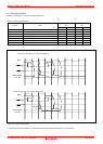
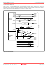
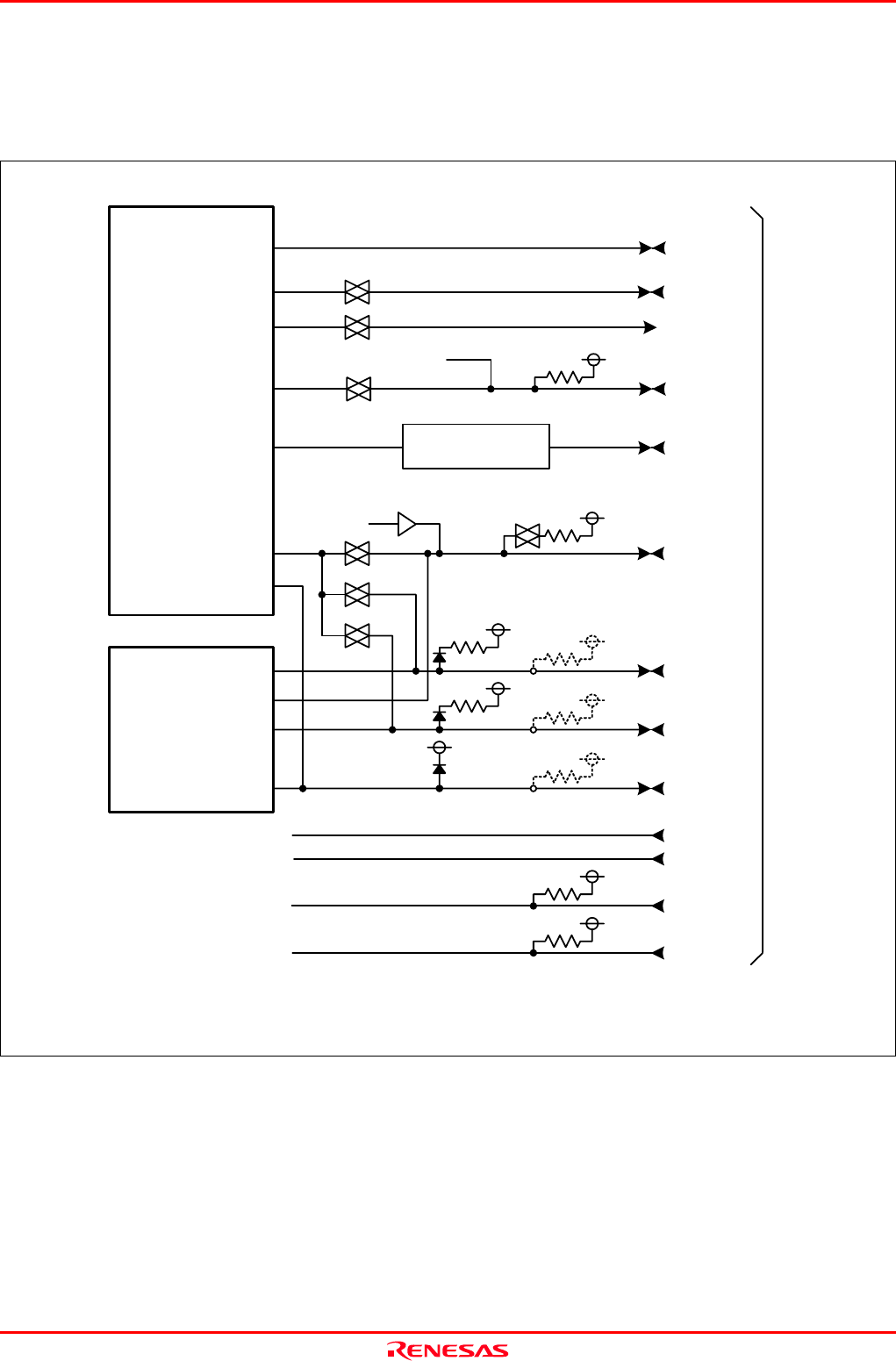
4.4 Connection Diagrams
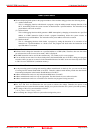
Figure 4.4 shows a connection diagram of the M306V8T-EPB. This connection diagram mainly show the circuit to be
connected to the user system. The circuits not connected to the user system such as the emulator’s control system are omitted.
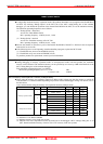
Tables 4.5 and 4.6 show IC electric characteristics of this product for reference purpose.
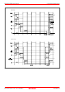
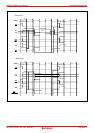
Figure 4.4 Connection diagram
IC3
M16C/6V8
I/O Emulate
P67--P60
P77--P70
P83,P82
P91,P90
P86/Xcout
P87/Xcin
P86/Xcout
P87/Xcin
CNVss1
BYTE
RESET*
Xin
74HC4066
74HC4066
510kΩ Vcc
510kΩ Vcc
*
*
*
*
IC4
P07--P00
51kΩ
Vcc
P27--P20
51kΩ
Vcc
AN7--AN3
74HC4066
74HC4066
51kΩ Vcc
P107--P103
74HC4066
74HC4066
7WH125
*
P17--P10
P37--P30
P47--P40
P57--P50
51kΩ
Vcc
*: Connected to the inside of the emulator.
Pullup registers in indicated by
dashed line: socket mounted.
R3:0Ω
Vcc
R2:0Ω
Vcc
Vcc
510kΩ Vcc
User system
Xout
74HC4066
Xout
P67--P60
P77--P70
P83,P82
P91,P90
*
Port Emulation
FPGA
P17--P15
OSD Signal
OSD SignalOSD circuit