


Si53xx-RM
Rev. 0.5 115
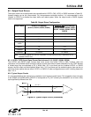
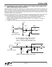
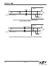
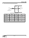
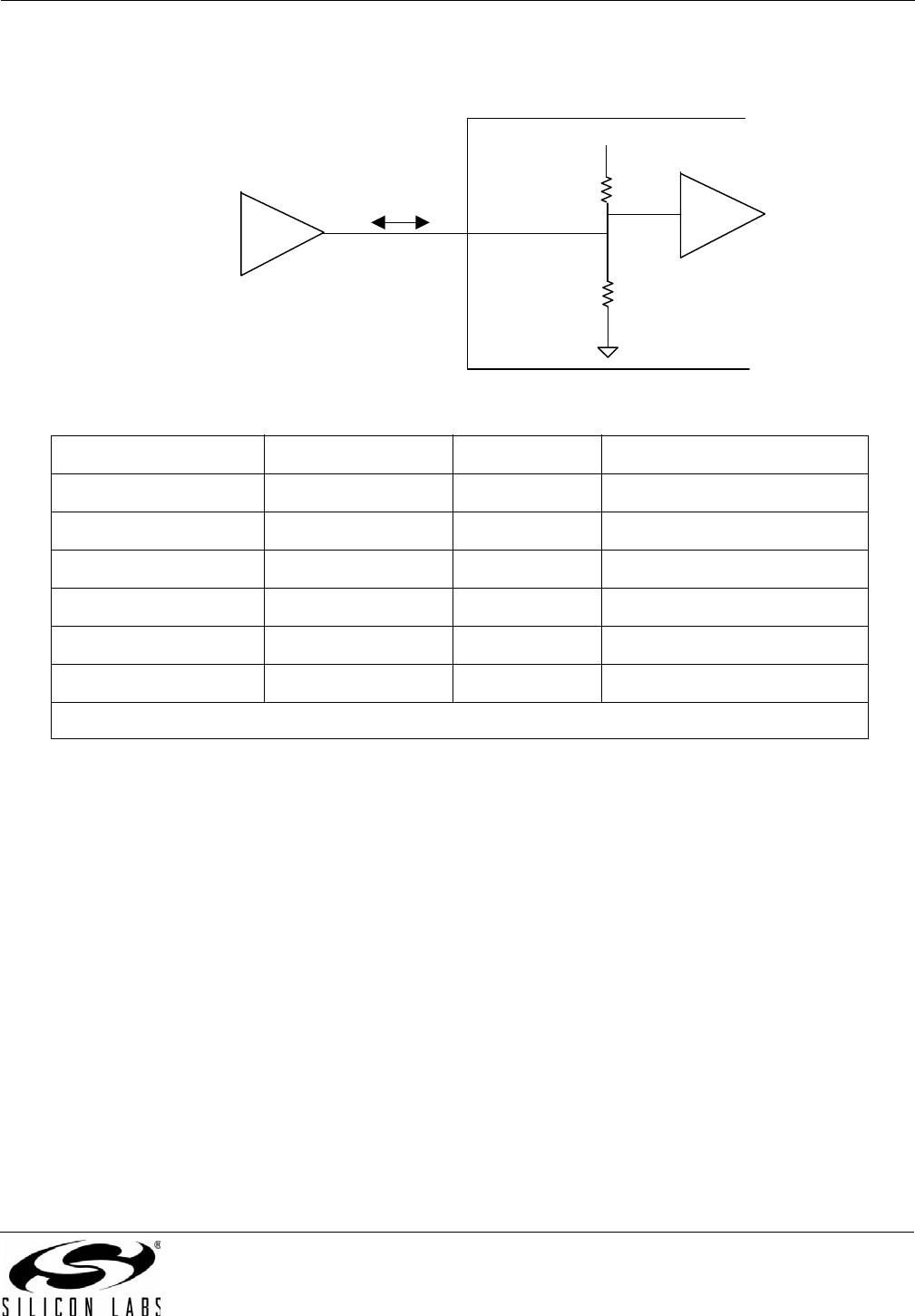
8.5. Three-Level (3L) Input Pins (No External Resistors)
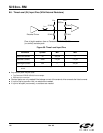
Figure 55. Three Level Input Pins
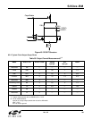
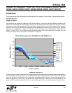
Parameter Symbol Min Max
Input Voltage Low Vill — .15 x V
DD
Input Voltage Mid Vimm .45 x Vdd .55 x V
DD
Input Voltage High Vihh .85 x Vdd —
Input Low Current Iill –6 µA —
Input Mid Current Iimm –2 µA 2 µA
Input High Current Iihh — 6 µA
Note: The above currents are the amount of leakage that the 3L inputs can tolerate from an external driver.
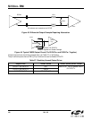
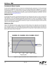
External Driver
Si53xx
I
imm
75 k
V
DD
75 k