


Si53xx-RM
Rev. 0.5 41
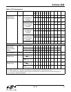
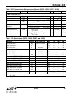
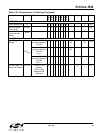
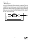
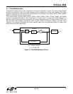
LVCMOS Pins
Input Capacitance C
in
—— 3pF
Minimum Reset
Pulse Width
t
RSTMN
1——µs
Reset to Micropro-
cessor Access
Ready
t
READY
——10ms
LVCMOS Output Pins
LOSn Trigger
Window
LOS
TRIG
From last CKIN_n
to internal detection
of LOSn
100 x
N3
—570 x
N3
T
CKIN
From last CKIN_n
to internal detection
of LOSn
0.8 x
N3
— 4.5 x N3 T
CKIN
From last CKIN_n
to internal detection
of LOSn
N3 = 1
250 ns — 4.5 T
CKIN
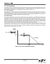
Time to Clear LOL
after LOS Cleared
t
CLRLOL
LOS to LOL
Assume
Fold = Fnew,
Stable XA/XB
reference
—10 —ms
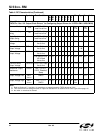
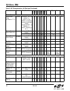
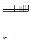
Table 8. AC Characteristics—All Devices (Continued)
Parameter
Symbol Test Condition
Si5316
Si5322
Si5324
Si5325
Si5365
Si5366
Si5367
Si5368
Min Typ Max Units
N3 1