


Si53xx-RM
Rev. 0.5 95
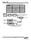
7.9. Output Clock Drivers (Si5319, Si5324, Si5325, Si5326, Si5327, Si5367, Si5368,
Si5369, Si5374, Si5375)
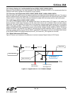
The device includes a flexible output driver structure that can drive a variety of loads, including LVPECL, LVDS,
CML, and CMOS formats. The signal format of each output is individually configurable through the
SFOUTn_REG[2:0] register bits, which modify the output common mode and differential signal swing.
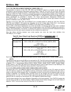
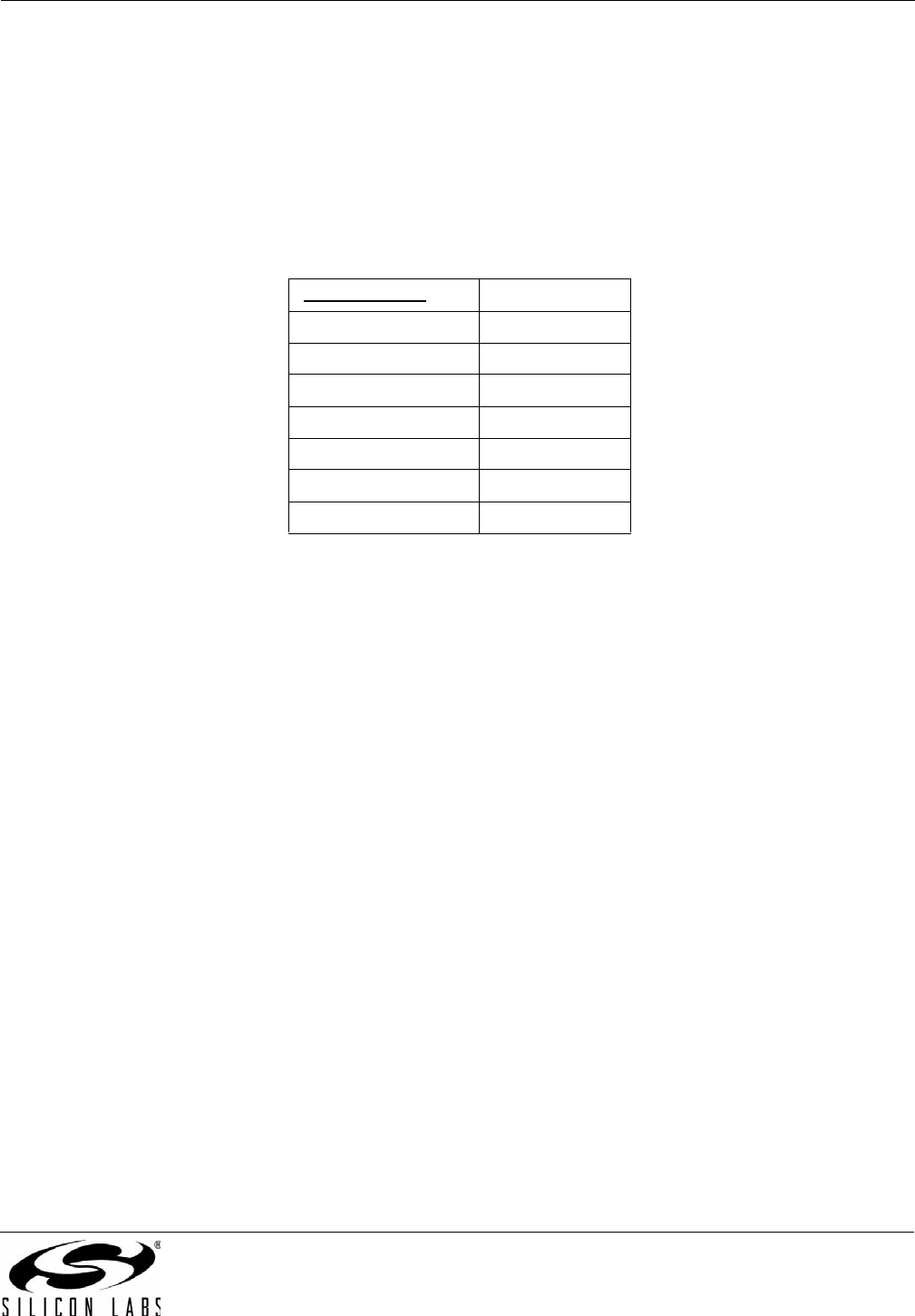
Table 47 shows the signal formats based on the supply voltage and the type of load being driven. For the CMOS
setting, both output pins drive single-ended in-phase signals and should be externally shorted together to obtain
the maximum drive strength.
The SFOUTn_REG[2:0] register bits can also be used to disable the outputs. Disabling the outputs puts the
CKOUT+ and CKOUT– pins in a high-impedance state relative to V
DD
(common mode tri-state) while the two
outputs remain connected to each other through a 200 on-chip resistance (differential impedance of 200 ). The
clock output buffers and DSPLL output dividers NCn are powered down in disable mode.
The additional functions of “Hold Logic 1” and “Hold Logic 0”, which create static logic levels at the outputs, are
available. For differential output buffer formats, the Hold Logic 1 state causes the positive output of the differential
signal to remain at its high logic level while the negative output remains at the low logic level. For CMOS output
buffer format, both outputs remain high during the Hold Logic 1 state. These functions are controlled by the
HLOG_n bits. When entering or exiting the “Hold Logic 1” or “Hold Logic 0” states, no glitches or runt pulses are
generated on the outputs. Changes to SFOUT or HLOG will change the output phase. An ICAL is required to re-
establish the output phase. When SFOUT = 010 for CMOS, bypass mode is not supported.
7.9.1. Disabling CKOUTn
Disabling CKOUTn output powers down the output buffer and output divider. Individual disable controls are
available for each output using the DSBLn_REG.
7.9.2. LVPECL TQFP Output Signal Format Restrictions at 3.3 V (Si5367, Si5368, Si5369)
The LVPECL and CMOS output formats draw more current than either LVDS or CML; therefore, there are
restrictions in the allowed output format pin settings that limit the maximum power dissipation for the TQFP devices
when they are operated at 3.3 V. When Vdd = 3.3 V and there are four enabled LVPECL or CMOS outputs, the fifth
output must be disabled. When Vdd = 3.3 V and there are five enabled outputs, there can be no more than three
outputs that are either LVPECL or CMOS. All other configurations are valid, including all with Vdd = 2.5 V.
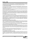
Table 47. Output Signal Format Selection
SFOUTn_REG[2:0] Signal Format
111 LVDS
110 CML
101 LVPECL
011 Low-swing LVDS
010 CMOS
000 Disabled
All Others Reserved